Photodiode and method for improving full-trap capacity and quantum efficiency of image sensor

A photodiode and image sensor technology, applied in circuits, electrical components, semiconductor devices, etc., can solve the problems of reducing the detectable light intensity range, dynamic range, signal-to-noise ratio and sensitivity, and deteriorating imaging quality, etc. The effect of electron transfer, increasing quantum efficiency, and increasing full well capacity

Active Publication Date: 2012-10-03
TIANJIN UNIV
View PDF6 Cites 22 Cited by
  • Summary
  • Abstract
  • Description
  • Claims
  • Application Information

AI Technical Summary

Problems solved by technology

Although this structure is mainstream in the design of large-size pixels, however, as the pixel size continues to shrink, the area of ​​a single pixel unit will gradually shrink, and the design of these small-size pixels will face some new problems with the size reduction: dynamic range, signal Key indicators such as noise ratio and sensitivity will be reduced to varying degrees due to the reduction in pixel size
These limiting factors will deteriorate the image quality and reduce the range of detectable light intensity to varying degrees

Method used


Image

  • Photodiode and method for improving full-trap capacity and quantum efficiency of image sensor
  • Photodiode and method for improving full-trap capacity and quantum efficiency of image sensor
  • Photodiode and method for improving full-trap capacity and quantum efficiency of image sensor

Examples


Embodiment Construction

[0023] The invention relates to an optimized structure of a photodiode (PD), which can enable small-sized pixels to achieve higher full-well capacity without degrading image tailing of pixel units.

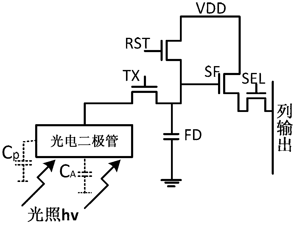
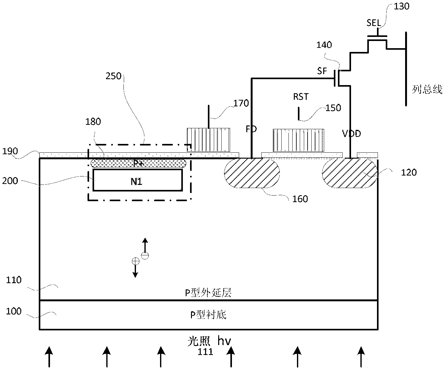
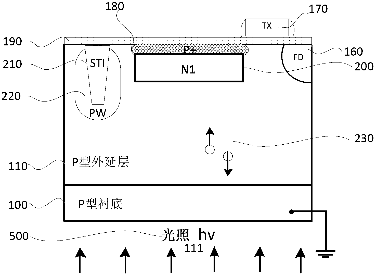
[0024] In the traditional back-illuminated clamped photodiode (PPD) structure, the N-buried layer 200 of the photodiode is realized by one-step N-type doping, such as figure 1 shown. With the shrinking of pixel size, the photodiode area of ​​a single pixel is also decreasing, and the area of ​​the N buried layer will be reduced accordingly. If this structure is still used, it will not be able to provide sufficient full well capacity for the pixel unit. And if in order to increase the full well capacity, only increase the implantation energy of the N buried layer 200 to make the N buried layer with a deeper vertical depth attempt to increase the full well capacity, this will make the N buried layer lack obvious vertical concentration gradient, causing far away Electrons inside the...


PUM


Abstract

The invention relates to a complementary metal oxide semiconductor (CMOS) solid image sensor, and particularly relates to a photodiode and a method for improving the full-trap capacity and the quantum efficiency of an image sensor. In order to ensure that the extended full-trap capacity can be fully used up so that the extension is not based on wasting the streaking performance of images, and fundamentally improve key performance indexes of pixel units, such as dynamic range, signal to noise ratio, and sensitivity. In order to achieve the objective the invention adopts the following technicalscheme: an N buried layer with a shallower depth is injected to a P type epitaxial layer, a high-concentration P+-doped clamping layer is arranged on the N buried layer, a second N buried layer is arranged under the N buried layer, and a longitudinal P insertion layer structure is formed from the interface of the second N buried layer and the P type epitaxial layer to the inner part of the N buried layer. The photodiode and the method provided by the invention is mainly applied to the design and manufacture of the image sensor.

Description

technical field [0001] The invention relates to a complementary metal oxide semiconductor (CMOS) solid-state image sensor, in particular to a photodiode structure and a manufacturing method for improving the full well capacity and quantum efficiency of the CMOS image sensor. Specifically, it relates to photodiodes and methods for improving the full well capacity and quantum efficiency of image sensors. Background technique [0002] In recent years, benefiting from the advancement of the standard CMOS process and the continuous improvement of the CMOS manufacturing process, CMOS image sensors have surpassed CCD image sensors to become the mainstream of solid-state image sensors, realizing the rapid development of CMOS image sensors in recent years. In the field of CMOS image sensors, with the help of the development of back-illuminated technology, the pixel unit size has been reduced by leaps and bounds: from 3um under the traditional front-illuminated technology to 0.7um und...

Claims


Application Information

Patent Timeline
Patent Type & Authority Applications(China)
IPC IPC(8): H01L27/146H01L31/102H01L31/0352H01L31/18
Inventor 徐江涛孙羽高静史再峰姚素英
Owner TIANJIN UNIV
Why Eureka
Try Eureka