Shared pixel structure applied to automatic focusing and image sensing device

A technology of sharing pixels and auto-focus, which is applied in the field of image sensors, can solve the problem of low full-well capacity of pixel units, and achieve the effect of increasing the area and increasing the full-well capacity

Pending Publication Date: 2022-07-01
思特威(上海)电子科技股份有限公司
View PDF0 Cites 0 Cited by
  • Summary
  • Abstract
  • Description
  • Claims
  • Application Information

AI Technical Summary

Problems solved by technology

[0004] However, in some working states, the camera system does not need auto-focus, but only works in normal mode (non-focus mode), so it is necessary to switch the camera system between auto-focus and normal mode. After normal mode, the full well capacity of the pixel unit is lower

Method used


Image

  • Shared pixel structure applied to automatic focusing and image sensing device
  • Shared pixel structure applied to automatic focusing and image sensing device
  • Shared pixel structure applied to automatic focusing and image sensing device

Examples


no. 1 example

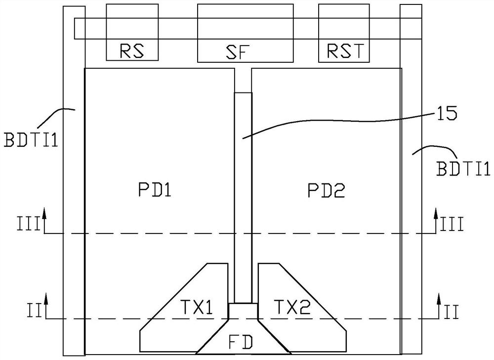
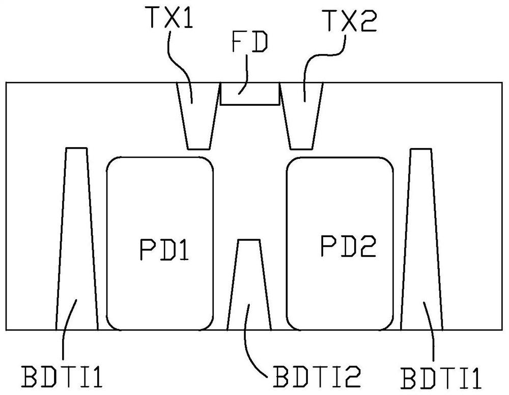
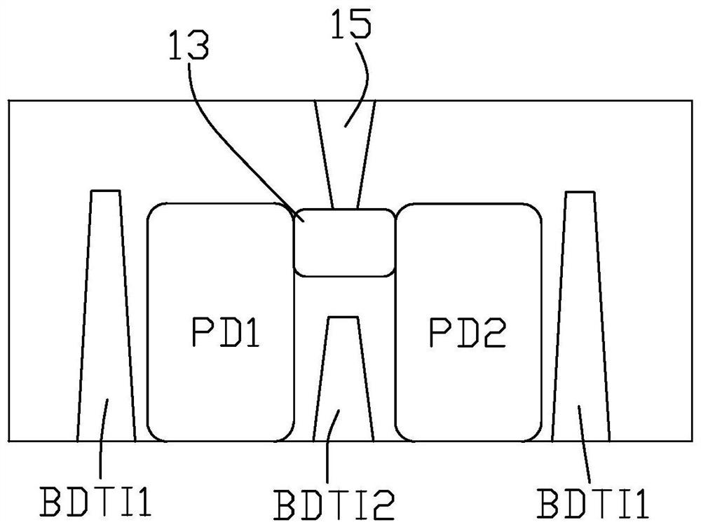
[0032] Please refer to Figure 1 to Figure 3 , figure 1 A schematic structural diagram of the shared pixel structure provided by the first embodiment of the present invention is shown, figure 2 shows along figure 1 Section II-II schematic diagram, image 3 shows along figure 1 Schematic cross-section of III-III. The shared pixel structure of this embodiment includes a first photodiode PD1, a second photodiode PD2, a first transfer transistor TX1, a second transfer transistor TX2, a floating diffusion FD, a reset transistor RST, a source follower transistor SF, and a selection transistor RS , the first photodiode PD1 and the first transfer transistor TX1 constitute the first photosensitive unit, the second photodiode PD2 and the second transfer transistor TX2 constitute the second photosensitive unit, and the first photosensitive unit and the second photosensitive unit share the floating diffusion point FD, Reset transistor RST, source follower transistor SF and select tr...

no. 2 example

[0046] The present invention also provides another embodiment of the shared pixel structure, such as Figure 5 and Image 6 As shown, the shared pixel structure of this embodiment includes four first photosensitive units and four second photosensitive units, and the first photosensitive units and the four second photosensitive units share the same reset transistor RST and the same source follower transistor SF and the same select transistor RS.

[0047] Specifically, four first photosensitive units and four second photosensitive units are arranged in a 2*2 manner. Specifically, the first transmission transistor TX1 and the second transmission transistor TX2 in the first row are disposed adjacent to the first transmission transistor TX1 and the second transmission transistor TX2 in the second row. Such an arrangement centrally arranges the first transmission transistor TX1 and the second transmission transistor TX2, so that the first photodiode PD1 and the second photodiode P...

no. 3 example

[0049] The present invention also provides a shared pixel structure of another embodiment, such as Figure 7 As shown, the shared pixel structure of this embodiment includes four first photosensitive units and four second photosensitive units, and the first photosensitive units and the four second photosensitive units share the same reset transistor RST and the same source follower transistor SF and the same select transistor RS.

[0050] Specifically, four first photosensitive units and four second photosensitive units are arranged in a 1*4 manner. Specifically, the first transmission transistor TX1 and the second transmission transistor TX2 in the first row are arranged adjacent to the first transmission transistor TX1 and the second transmission transistor TX2 in the second row, and the first transmission transistor TX1 and the second transmission transistor in the third row are arranged adjacent to each other. The transfer transistor TX2 is disposed adjacent to the first ...


PUM


Abstract

The invention discloses a shared pixel structure applied to automatic focusing and an image sensing device, and the structure comprises a first photodiode, a second photodiode, a first transmission transistor, a second transmission transistor, a floating diffusion point, a reset transistor, a source electrode following transistor, and a selection transistor. The first photodiode and the second photodiode are arranged at an interval, a connecting part is arranged between the first photodiode and the second photodiode, the shared pixel structure further comprises a control part, and the control part is used for controlling the connecting part to connect or disconnect the first photodiode and the second photodiode. According to the shared pixel structure and the image sensing device, the connecting part is arranged between the first photodiode and the second photodiode, so that the first photodiode and the second photodiode are connected or disconnected; the connecting part connecting the first photodiode and the second photodiode can increase the area of the whole photoelectric induction, so that the full well capacity is increased.

Description

technical field [0001] The present invention relates to the technical field of image sensors, and in particular, to a shared pixel structure and an image sensing device capable of automatic focusing. Background technique [0002] An image sensor is a device that converts optical image information into electrical information. TOF (Time of Fly) is mainly used in image sensors for systems that acquire 3D images. The system measures the distance from the imaging target to the image sensing device using the time it takes for the light to travel from the light source to the object and reflect back to the image sensor based on the optical time of flight. Each pixel of the image sensor participates in ranging to obtain high-precision depth images. [0003] Currently, camera systems require autofocus (AF) in many applications to ensure that relevant parts of the scene at varying distances from the camera are captured as an in-focus image plane. An image sensor that acquires informa...

Claims


Application Information

Patent Timeline
Patent Type & Authority Applications(China)
IPC IPC(8): H04N5/369H01L27/146
CPCH01L27/14612H01L27/14643H04N25/705
Inventor 张盛鑫徐辰
Owner 思特威(上海)电子科技股份有限公司
Why Eureka
Try Eureka