Image sensor and formation method thereof

An image sensor and device technology, applied in the direction of electric solid state devices, semiconductor devices, electrical components, etc., can solve the problems of reduced absorption coefficient, low long-wave light absorption rate, low quantum efficiency, etc., and achieve the effect of improving convenience.

Inactive Publication Date: 2019-10-25
HUAIAN IMAGING DEVICE MFGR CORP
View PDF4 Cites 1 Cited by
  • Summary
  • Abstract
  • Description
  • Claims
  • Application Information

AI Technical Summary

Problems solved by technology

[0003] Especially in front-side illumination (FSI) CIS, the quantum efficiency of absorbing long-wavelength light is relatively low, because the absorption coefficient of the semiconductor substrate (such as a silicon substrate) decreases with the increase of the wavelength of the incident light, For example, absorbing 700nm light in silicon requires a 5um absorption path
Therefore, when absorbing long-wave light, most of the light will pass through the photodiode (Photo Diode, PD) area, resulting in a low absorption rate for long-wave light

Method used


Image

  • Image sensor and formation method thereof
  • Image sensor and formation method thereof
  • Image sensor and formation method thereof

Examples


Embodiment Construction

[0023] As mentioned above, in existing image sensors, the quantum efficiency of absorbing long-wave light is relatively low, so when absorbing long-wave light, most of the light will penetrate the photodiode region, affecting the quantum efficiency and full well capacity.

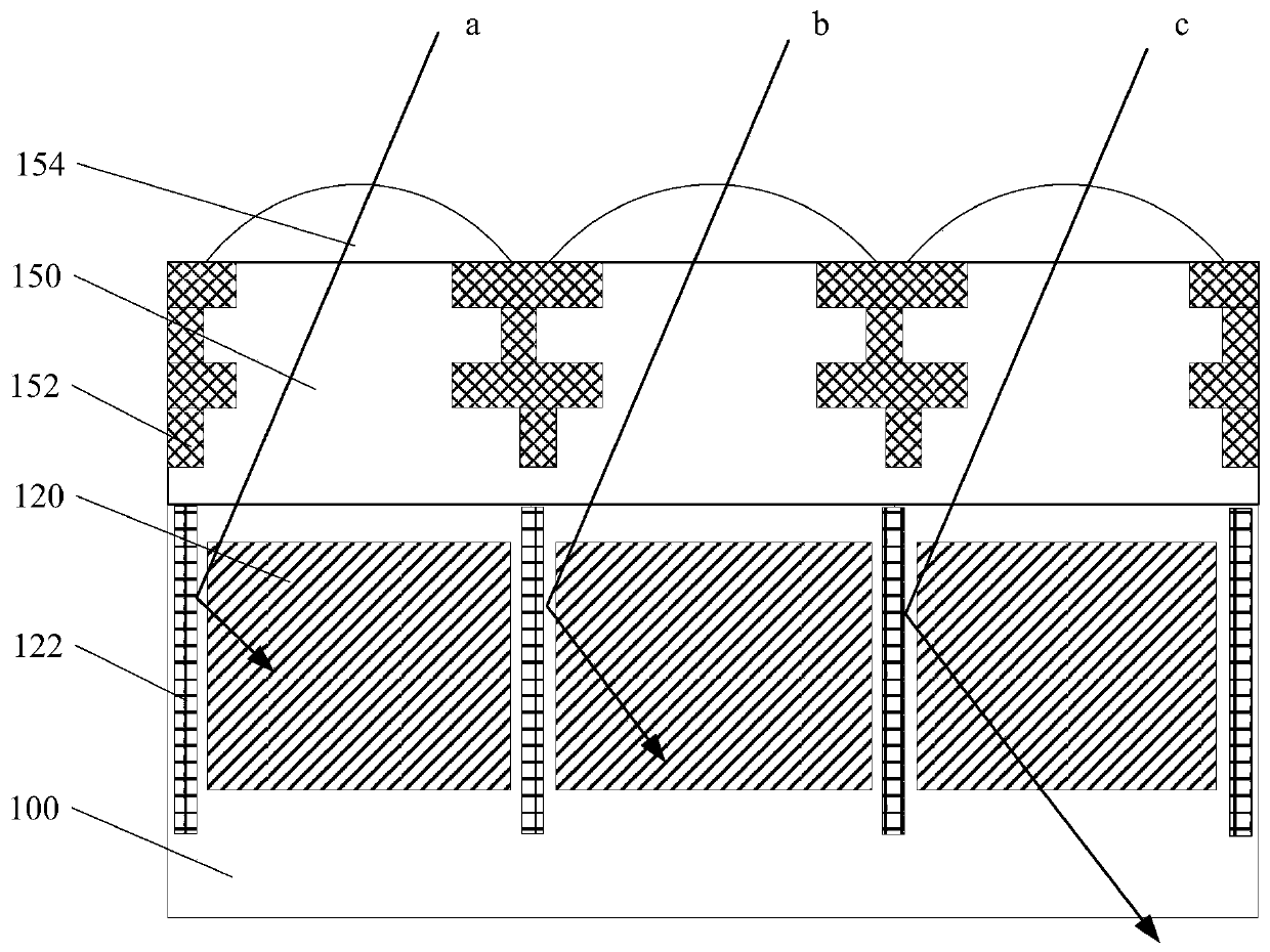
[0024] refer to figure 1 , figure 1 It is a schematic cross-sectional structure diagram of an image sensor in the prior art.

[0025] The image sensor may include a semiconductor substrate 100 , an isolation structure 122 and a photodiode 120 .

[0026] Wherein, the isolation structure 122 is located in the semiconductor substrate 100 for isolating adjacent photodiodes 120 , and the photodiodes 120 are also located in the semiconductor substrate 100 .

[0027] On the surface of the semiconductor substrate 100 , the image sensor may further include a metal interconnection layer 150 , and the metal interconnection layer 150 may contain a metal interconnection structure 152 .

[0028] On the surface of the ...


PUM


Abstract

The invention relates to an image sensor and a formation method thereof. The method comprises steps that a first semiconductor substrate and a second semiconductor substrate are provided; a reflectionstructure is formed on a front surface of the first semiconductor substrate and / or a front surface of the second semiconductor substrate; the front surface of the first semiconductor substrate and the front surface of the second semiconductor substrate are bonded; a pixel device is formed on a back surface of the first semiconductor substrate or a back surface of the second semiconductor substrate, and the pixel device includes photodiodes; light penetrating at least a part of the photodiodes is reflected by the reflection structure to at least a part of the photodiodes. The method is advantaged in that the transmitted light can be absorbed in a secondary time, and the absorbing capacity of the incident light is enhanced.

Description

technical field [0001] The invention relates to the technical field of semiconductor manufacturing, in particular to an image sensor and a forming method thereof. Background technique [0002] Image sensors (Image Sensors) are the core components of camera equipment, which realize the image capture function by converting optical signals into electrical signals. Since the CMOS image sensor (CMOS Image Sensor, CIS) has the advantages of low power consumption and high signal-to-noise ratio, it has been widely used in various fields. [0003] Especially in front-side illumination (FSI) CIS, the quantum efficiency of absorbing long-wavelength light is relatively low, because the absorption coefficient of the semiconductor substrate (such as a silicon substrate) decreases with the increase of the wavelength of the incident light, For example, absorbing 700nm light in silicon requires a 5um absorption path. Therefore, when absorbing the long-wave light, most of the light will pas...

Claims


Application Information

Patent Timeline
Patent Type & Authority Applications(China)
IPC IPC(8): H01L27/146
CPCH01L27/14629H01L27/14685H01L27/1469
Inventor 柯天麒刘少东
Owner HUAIAN IMAGING DEVICE MFGR CORP
Why Eureka
Try Eureka