Supercharge Your Innovation With Domain-Expert AI Agents!

Surface-roughened double-layer adhesive structure LED light source and manufacturing method thereof

A LED light source and surface roughening technology, which is applied to electrical components, electrical solid devices, circuits, etc., can solve the problems of phosphor temperature rise, luminous efficiency reduction, phosphor quantum efficiency attenuation, etc., to improve the light output rate and improve The effect of the reflection effect

Inactive Publication Date: 2012-10-03
SUNSUN LIGHTING CHINA
View PDF4 Cites 11 Cited by
  • Summary
  • Abstract
  • Description
  • Claims
  • Application Information

AI Technical Summary

Problems solved by technology

As far as the current COB integrated packaging light source is concerned, the basic process is to integrate and package multiple chips on a small aluminum substrate, and then coat the phosphor and silica gel mixture on the chip, so as to manufacture the COB integrated packaging light source. Although the process is simple, the existing problems are obvious: after the light source works normally, the chip will continue to heat up, part of the heat will be conducted to the heat sink through the aluminum substrate or directly into the air, and part of the heat will be on the surface of the chip and the phosphor, The aggregation of silica gel will cause the temperature of the phosphor to rise significantly, which will cause the quantum efficiency of the phosphor to decay continuously, so that the luminous efficiency of the light source will gradually decrease after working for a long time. Therefore, it is necessary to design and manufacture the light source. Considering the influence of the heat of the chip on the phosphor

Method used


Image

  • Surface-roughened double-layer adhesive structure LED light source and manufacturing method thereof
  • Surface-roughened double-layer adhesive structure LED light source and manufacturing method thereof
  • Surface-roughened double-layer adhesive structure LED light source and manufacturing method thereof

Examples


Embodiment Construction

[0018] The present invention will be described in further detail below in conjunction with the accompanying drawings:

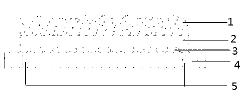
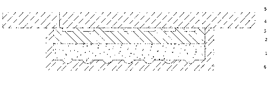
[0019] As shown in the figure: a double-layer glue structure LED light source with rough surface, including phosphor coating 1, transparent glue coating 2, chip 3, aluminum substrate 4, and through hole 5.

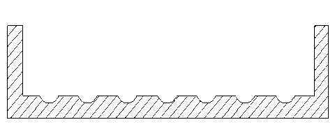
[0020] The chip 3 is fixed on the aluminum substrate 4, the transparent glue coating 2 covers the chip 3 and the aluminum substrate 4, and the phosphor coating 1 covers the transparent glue coating 2; a number of through holes are arranged on the aluminum substrate 4 5. The surface of phosphor coating 1 is uneven and rough. The surface of the aluminum substrate 4 is a silver-plated layer or mirror aluminum.

[0021] The manufacturing method of the double-layer glue structure LED light source with rough surface is as follows:

[0022] There are two through holes on the aluminum substrate, one of which is a glue injection hole and the other is an air circulation h...


PUM


Abstract

The invention relates to a surface-roughened double-layer adhesive structure LED light source and a manufacturing method thereof and belongs to the field of semiconductor illumination. Chips are fixed on an aluminum substrate; a transparent adhesive coating covers the chip and the aluminum substrate; a fluorescent powder coating covers the transparent adhesive coating layer; a plurality of through holes are formed on the aluminum substrate; and the surface of the fluorescent powder coating layer is concave-convex rough surface. The manufacturing method comprises the following manufacturing steps: fixing the chips, treating a mould, injecting an adhesive layer, and solidifying and forming. Compared with the prior art, the surface-roughened double-layer adhesive structure LED light source and the manufacturing method thereof have the beneficial effects that in the surface-roughened double-layer adhesive structure LED light source, a silica gel layer is spaced between fluorescent powder and the chips, so that the effect of chip heating on the fluorescent powder is remarkably reduced, and the stability of the fluorescent powder can be remarkably improved; and meanwhile, when the fluorescent powder coating and an air contact surface are roughened, the total reflection ratio of light transmitted from silica gel to air is reduced, and the luminous flux of the light source is directly improved.

Description

technical field [0001] The invention relates to a surface-roughened double-layer adhesive structure LED light source and a manufacturing method, belonging to the field of semiconductor lighting. Background technique [0002] At present, in the field of semiconductor lighting, improving light efficiency and improving heat dissipation are two main research focuses, and there is a mutual influence between these two factors, especially the heat dissipation effect obviously affects the stability of each component. As far as the current COB integrated packaging light source is concerned, the basic process is to integrate and package multiple chips on a small aluminum substrate, and then coat the phosphor and silica gel mixture on the chip, so as to manufacture the COB integrated packaging light source. Although the process is simple, the existing problems are obvious: after the light source works normally, the chip will continue to heat up, part of the heat will be conducted to th...

Claims


Application Information

Patent Timeline
IPC IPC(8): H01L33/54H01L33/50H01L25/075H01L33/00
Inventor 冼钰伦张伟张瑞西江新光
Owner SUNSUN LIGHTING CHINA
Features
  • R&D
  • Intellectual Property
  • Life Sciences
  • Materials
  • Tech Scout
  • Unparalleled Data Quality
  • Higher Quality Content
  • 60% Fewer Hallucinations
Learn More