Fully-automatic loading and unloading device used in processing semiconductor chips by laser and application method thereof

A laser processing and semiconductor technology, which is applied in the field of fully automatic loading and unloading devices for laser processing semiconductor wafers, can solve problems such as poor operating efficiency and scrap rate, and achieve the effects of quality assurance, simple operation, and shortened loading and unloading time

Active Publication Date: 2014-08-20
HEFEI ZHICHANG PHOTOELECTRIC TECH
View PDF5 Cites 0 Cited by
  • Summary
  • Abstract
  • Description
  • Claims
  • Application Information

AI Technical Summary

Problems solved by technology

[0003] The technical problem to be solved by the present invention is to provide a fully automatic loading and unloading device for laser processing semiconductor wafers and its use method, which solves the problems of manual loading and unloading operations in existing processing, poor operating efficiency, and scrap rate during operation

Method used


Image

  • Fully-automatic loading and unloading device used in processing semiconductor chips by laser and application method thereof
  • Fully-automatic loading and unloading device used in processing semiconductor chips by laser and application method thereof

Examples


Embodiment Construction

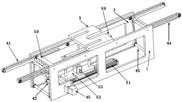
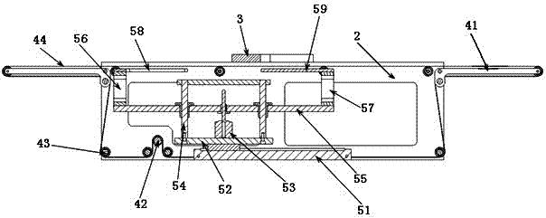
[0025] See figure 1 , figure 2 , a fully automatic loading and unloading device for laser processing semiconductor wafers, including a support frame composed of a front end plate 1 and a rear end plate 2, an M-shaped laser processing platform 3 arranged on the top of the support frame, arranged on the support frame and located at The wafer transmission mechanism below the M-shaped laser processing platform 3 and the linkage loading and unloading mechanism arranged in the support frame and below the wafer transmission mechanism;

[0026] The wafer transfer mechanism includes an idler arm 41 arranged at the top ends of the front end plate 1 and the rear end plate 2 and positioned below the level of the M-shaped laser processing platform 3, and a pulley set 42 connected between the front end plate 1 and the rear end plate 2 And idler group 43, the transmission belt 44 that is wound on pulley group 42, idler group 43 and idler arm 41 and the transmission driving device 45 that d...


PUM


Abstract

The invention discloses a fully-automatic loading and unloading device used in processing semiconductor chips by laser and an application method thereof. The fully-automatic loading and unloading device used in processing semiconductor chips by laser comprises a support frame, a laser processing platform, a chip transmission mechanism, and a linkage loading and unloading mechanism, wherein the laser processing platform is arranged on the top end of the support frame, the chip transmission mechanism is arranged on the support frame and located below the laser processing platform, and the linkage loading and unloading mechanism is arranged in the support frame and located below the chip transmission mechanism. The fully-automatic loading and unloading device of the invention has the advantages that human operation is not needed in loading and unloading processes and the loading and unloading processes are performed simultaneously, which improves production efficiency and rate of finished products, avoids pollution to the chips caused by direct contact of workers with the chips, improves the quality of the products, realizes seamless linkage between the current working procedure and the previous and the next working procedures at the same time, and omits a step of workpiece transportation by human labor between two working procedures.

Description

technical field [0001] The invention relates to the field of semiconductor wafer laser processing, in particular to a fully automatic loading and unloading device for laser processing semiconductor wafers and a method for using the same. Background technique [0002] In recent years, with the promotion and application of laser processing technology, laser processing equipment has been widely used in the field of semiconductor wafer manufacturing. Especially in the field of photovoltaic cells, the application of laser technology has greatly improved the production efficiency and quality of solar cells, and at the same time reduced the production and manufacturing costs of solar cells to a large extent. However, at present, most of the laser processing equipment for semiconductor wafers, including photovoltaic cells, still use a semi-automatic method of manual loading and unloading, which has the following shortcomings that need to be improved urgently: 1. Generally, two opera...

Claims


Application Information

Patent Timeline
Patent Type & Authority Patents(China)
IPC IPC(8): H01L21/677B23K26/70
Inventor 翟骥吴周令
Owner HEFEI ZHICHANG PHOTOELECTRIC TECH
Why Eureka
Try Eureka