Substrate for photomask, photomask, method for manufacturing photomask and method for transfering pattern

A manufacturing method and pattern transfer technology, which are used in microlithography exposure equipment, semiconductor/solid-state device manufacturing, optics, etc., can solve problems such as deterioration, color turbidity, and poor liquid crystal display devices, and achieve improved transfer accuracy. The effect of improving coordinate accuracy

Active Publication Date: 2012-10-17
HOYA CORP
View PDF9 Cites 4 Cited by
  • Summary
  • Abstract
  • Description
  • Claims
  • Application Information

AI Technical Summary

Problems solved by technology

[0012] However, the inventors of the present application have found that even if this method is useful for alleviating the influence of the deflection of the photomask on the pattern transfer, it is still not enough to manufacture a precision display device for the above-mentioned use using only this method. fully
[0013] For example, it has been found that when performing the above-mentioned proximity exposure, although the formation accuracy of the transfer pattern that the photomask has is sufficiently high and within the reference range, the transfer pattern formed on the transfer target Insufficient superimposition accuracy may cause malfunction of the liquid crystal display device, cloudy color, etc.
As liquid crystal display devices continue to be refined, such deterioration in pattern superimposition accuracy cannot be tolerated.

Method used


Image

  • Substrate for photomask, photomask, method for manufacturing photomask and method for transfering pattern
  • Substrate for photomask, photomask, method for manufacturing photomask and method for transfering pattern
  • Substrate for photomask, photomask, method for manufacturing photomask and method for transfering pattern

Examples


Embodiment approach

[0050] An embodiment of the present invention will be described below.

[0051] (1) Manufacturing process of color filter

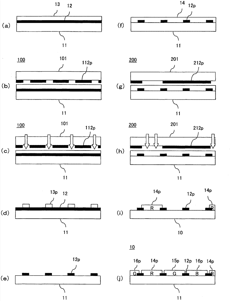
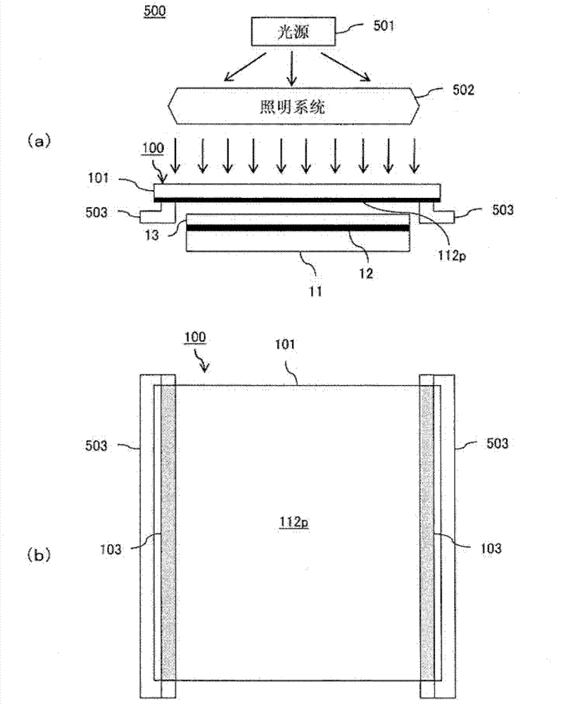
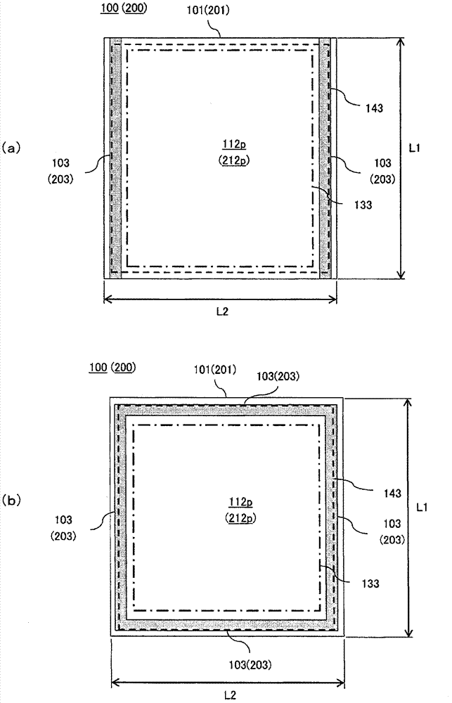
[0052] First, refer to Figure 1 ~ Figure 3 The manufacturing process of a color filter used in a liquid crystal display device etc. is demonstrated. figure 1 It is a flowchart illustrating the outline of the manufacturing process of the color filter of this embodiment. figure 2 (a) is a side view exemplifying a case where proximity exposure is performed in the manufacturing process of the color filter of this embodiment. figure 2 (b) is its top view. image 3 (a) is a plan view illustrating the planar structure of the photomask of this embodiment, image 3 (b) is a plan view illustrating a modification example thereof.

[0053] Such as figure 1 As shown, the color filter 10 for a liquid crystal display device is manufactured by sequentially performing the following steps: a black matrix layer 12p (which constitutes a color boundary portion) is formed on one m...


PUM


Abstract

The invention provides a substrate for a photomask, the photomask, a method for manufacturing the photomask and a method for transfering a pattern, and transferring precision of the pattern is improved in proximity exposure. The photomask is provided with: a transparent substrate; and a transferring pattern formed by composing a shading film formed at the surface of the transparent substrate to be a predetermined transferring pattern, wherein, a worktable using a depicting machine supports the second main surface of the transparent substrate from the lower part; and the transferring pattern is formed, for the flatness of the second main surface of the transparent surface when no supporting part is sued to support the transparent substrate from the lower part, when the height difference between each arbitrary two points, is disposed to be Delta Zb([mu]m), Delta Zb<=(1/T)*3.0.

Description

Technical field [0001] The present invention relates to a substrate for a photomask, a photomask, a method for manufacturing a photomask, and a pattern transfer method. Background technique [0002] A liquid crystal display device such as a computer or a portable terminal has the following structure: a TFT substrate (hereinafter also referred to as TFT) on which a TFT (thin film transistor) array is formed on a light-transmitting substrate and a transparent substrate Color filters with RGB patterns formed on them are pasted together, and liquid crystals are sealed between them. The color filter (hereinafter also referred to as CF) is manufactured by sequentially implementing the following steps: forming a black matrix layer constituting a color boundary on one main surface of a translucent substrate; A step of forming color filter layers (hereinafter also referred to as color layers) such as a red filter layer, a green filter layer, and a blue filter layer on one main surface of...

Claims


Application Information

Patent Timeline
Patent Type & Authority Applications(China)
IPC IPC(8): G03F1/60G03F7/00G03F7/20G02B5/20
CPCG03F1/22G03F1/26G03F1/32G03F1/46G03F1/60H01L21/0337G03F1/62
Inventor 土屋雅誉池边寿美
Owner HOYA CORP
Why Eureka
Try Eureka