Output buffer of source driver
An output buffer, source driver technology, applied in amplifiers, instruments, amplifiers with semiconductor devices/discharge tubes, etc., can solve the voltage slew rate imbalance, NMOS source tracker is not sensitive, affects thin film transistors LCD display visual performance and other issues
- Summary
- Abstract
- Description
- Claims
- Application Information
AI Technical Summary
Problems solved by technology
Method used
Image

Examples
Embodiment Construction
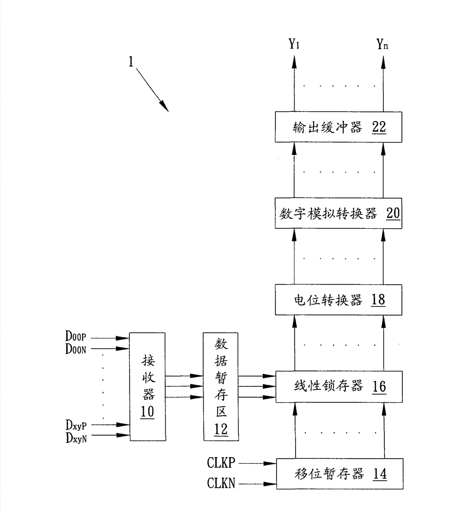
[0044] A specific embodiment according to the present invention is an output buffer. In this embodiment, the output buffer is applied in a source driver of a TFT-LCD display device, but not limited thereto.
[0045] In this embodiment, the circuit structure of the source driver of the thin film transistor liquid crystal display device also please refer to figure 1 . Such as figure 1As shown, the source driver 1 includes a receiver (receiver) 10, a data register (data register) 12, a bi-directional shift register (bi-directional shift register) 14, a linear latch (line latch) 16. A level shifter (level shifter) 18 , a digital-to-analog converter (Digital-to-Analog Converter) 20 and an output buffer (output buffer) 22 . Wherein, the receiver 10 is coupled to the data temporary register 12; the data temporary register 12 is coupled to the linear latch 16; the shift register 14 is coupled to the linear latch 16; the linear latch 16 is coupled to to the potential converter 18 ;...
PUM
 Abstract
Description
Claims
Application Information
 - R&D
- Intellectual Property
- Life Sciences
- Materials
- Tech Scout
- Unparalleled Data Quality
- Higher Quality Content
- 60% Fewer Hallucinations
Browse by: Latest US Patents, China's latest patents, Technical Efficacy Thesaurus, Application Domain, Technology Topic, Popular Technical Reports.
© 2025 PatSnap. All rights reserved.Legal|Privacy policy|Modern Slavery Act Transparency Statement|Sitemap|About US| Contact US: help@patsnap.com