Solid body shooting device and electronic device

A solid-state imaging device and semiconductor technology, applied in the direction of electric solid-state devices, semiconductor devices, radiation control devices, etc., can solve the problem of photoelectric conversion film sensitivity reduction and achieve high photoelectric conversion efficiency

Inactive Publication Date: 2012-10-17
SONY CORP
View PDF5 Cites 0 Cited by
  • Summary
  • Abstract
  • Description
  • Claims
  • Application Information

AI Technical Summary

Problems solved by technology

However, when the film thickness of the photoelectric conversion film becomes thinner, since the optical path length in the photoelectric conversion film becomes shorter, the sensitivity of the photoelectric conversion film decreases

Method used


Image

  • Solid body shooting device and electronic device
  • Solid body shooting device and electronic device
  • Solid body shooting device and electronic device

Examples


Embodiment Construction

[0020] Embodiments for realizing the technology of the present invention will be specifically described below with reference to the drawings. In addition, description will be made in the following order.

[0021] 1. Description of the embodiment

[0022] 1-1. The first example

[0023] 1-2. The second example

[0024] 1-3. The third example

[0025] 2. Modification

[0026] 3. Electronic devices (camera equipment)

[0027] 1. Description of the embodiment

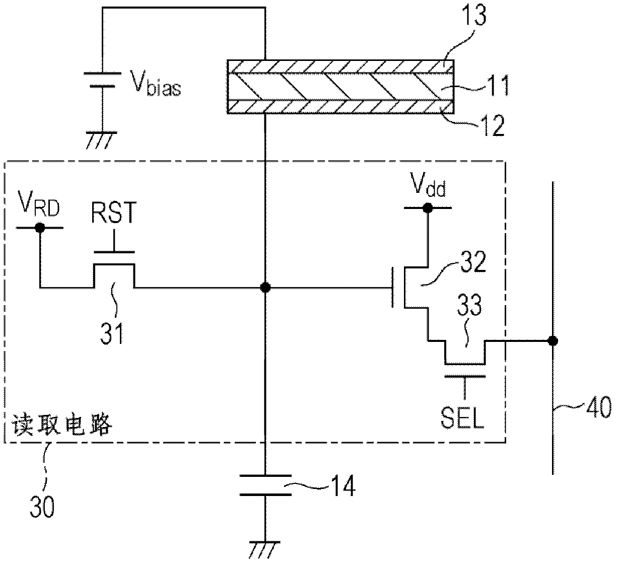
[0028] In the solid-state imaging device according to the embodiment of the present invention, incident light is photoelectrically converted using a photoelectric conversion film in a pixel unit. The photoelectric conversion film is disposed between two transparent electrodes outside the semiconductor substrate. In addition, charges obtained by photoelectric conversion of the photoelectric conversion film are taken out through one of the two transparent electrodes, and the charges are accumulated in a charge storage ...


PUM


Abstract

The invention relates to a solid body shooting device and an electronic device having the same. The solid body shooting device comprises a photoelectric conversion film which is disposed outside of a semiconductor substrate and between two transparent electrodes. The surface of the photoelectric conversion film is disposed in a manner of inclining with respect to the front surface of the semiconductor substrate. High photoelectric conversion efficiency can be achieved without reducing the sensitivity of the photoelectric conversion film.

Description

[0001] Cross References to Related Applications [0002] The present application contains subject matter related to the disclosure of Japanese Priority Patent Application JP 2011-073925 filed in the Japan Patent Office on Mar. 30, 2011, the entire content of which is hereby incorporated by reference. technical field [0003] The present invention relates to a solid-state imaging device and an electronic device, and more particularly, to a solid-state imaging device that photoelectrically converts incident light using a photoelectric conversion layer, and an electronic device including the solid-state imaging device. Background technique [0004] Generally, a solid-state imaging device has a structure in which incident light is photoelectrically converted in a photoelectric conversion unit formed in a semiconductor substrate, and imaging is performed by reading charges obtained by photoelectric conversion of the photoelectric conversion unit. In such solid-state imaging devic...

Claims


Application Information

Patent Timeline
Patent Type & Authority Applications(China)
IPC IPC(8): H01L27/146H04N5/372H04N5/374
CPCH01L27/14636H01L27/1464
Inventor 中泽正志平野智之
Owner SONY CORP
Why Eureka
Try Eureka