Supercharge Your Innovation With Domain-Expert AI Agents!

Three-layer anti-counterfeit label pcb board and its preparation process

A technology for PCB boards and anti-counterfeiting labels, which is applied to printed circuits connected with non-printed electrical components, printed circuits assembled with electrical components, etc. It can solve the problem that surface treatment cannot be gold-plated, cannot be fixed accurately, and three-layer boards cannot Accuracy and other issues to achieve the effect of reducing costs

Active Publication Date: 2016-06-22
KUSN HUACHEN ELECTRONICS
View PDF4 Cites 0 Cited by
  • Summary
  • Abstract
  • Description
  • Claims
  • Application Information

AI Technical Summary

Problems solved by technology

[0002] At present, the core technology of anti-counterfeiting labels is mainly chip binding, so the chip binding position is required to be very precise, while the traditional three-layer board cannot meet the required accuracy and cannot be fixed accurately
In addition, the traditional process of manufacturing three-layer PCB boards, due to the formation of 0.3mm deep pits between the pads and the board surface, the surface treatment (chemical gold plating) process cannot be partially gold-plated

Method used


Image

  • Three-layer anti-counterfeit label pcb board and its preparation process

Examples


Embodiment Construction

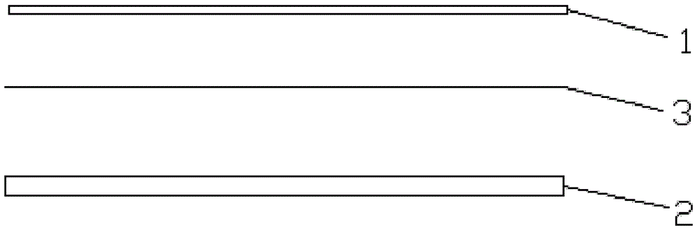
[0022] A three-layer anti-counterfeiting label PCB board, which includes a light board 1 and a core board 2 arranged in parallel to each other, ink and lines are printed on both sides of the core board, and a parallel arrangement is also arranged between the light board and the core board. There is an insulating layer 3 .

[0023] The insulating layer is made of epoxy glass cloth material.

[0024] The light board is made of glass fiber material.

[0025] A preparation process for a three-layer anti-counterfeit label PCB board, which comprises the following steps:

[0026] ① Core board cutting, that is, cutting the substrate into a core board of a set size according to needs;

[0027] ② Drill and hole the core board;

[0028] ③ Set up lines on both sides of the core board;

[0029] ④Electroplating the core board, that is, copper-plating the entire core board;

[0030] ⑤ Etching the core board, that is, displaying the circuit diagram required on the surface of the core boa...


PUM


Abstract

The invention discloses a three-layer anti-fake label PCB plate and a preparation process thereof. The PCB plate includes a light panel and a core plate which are arranged in a mutually parallel way. Surfaces of two sides of the core plate are printed with ink and a line respectively. An insulation layer is parallelly arranged between the light panel and the core plate. The preparation process can satisfy an accuracy requirement of a chip binding position, overall gilding is available for surface processing, the core plate is added with a resistance welding ink coating layer, and cost of the surface processing (chemical gilding) can be greatly reduced.

Description

technical field [0001] The invention relates to a PCB board, in particular to a three-layer anti-counterfeiting label PCB board and a preparation process thereof. Background technique [0002] At present, the core technology of the anti-counterfeiting label is mainly chip bonding, so the chip bonding position is required to be very precise, while the traditional three-layer board cannot meet the required accuracy and cannot be fixed precisely. In addition, the traditional process of manufacturing three-layer PCB boards, due to the formation of 0.3mm deep pits between the pads and the board surface, the surface treatment (chemical gold plating) process cannot be partially gold-plated. Contents of the invention [0003] In order to overcome the above-mentioned defects, the present invention provides a three-layer anti-counterfeit label PCB board and its preparation process. This process can not only meet the accuracy requirements of the chip binding position, but also the su...

Claims


Application Information

Patent Timeline
IPC IPC(8): H05K1/18H05K3/34
Inventor 孟文明
Owner KUSN HUACHEN ELECTRONICS
Features
  • R&D
  • Intellectual Property
  • Life Sciences
  • Materials
  • Tech Scout
  • Unparalleled Data Quality
  • Higher Quality Content
  • 60% Fewer Hallucinations
Learn More