Cross waveguide based on linear tapered multimode interference principle

A multi-mode interference and crossover technology, applied in the field of optical communication, can solve problems such as crosstalk, difficult manufacturing, and large insertion loss, and achieve the effects of low crosstalk, improved optical path integration, and low scattering loss

Active Publication Date: 2012-10-24
ZHEJIANG UNIV OF TECH
View PDF4 Cites 24 Cited by
  • Summary
  • Abstract
  • Description
  • Claims
  • Application Information

AI Technical Summary

Problems solved by technology

[0003] In order to overcome the problems of large insertion loss and serious crosstalk in the cross waveguide structure in the prior art, as well as the shortcomings of large structure

Method used


Image

  • Cross waveguide based on linear tapered multimode interference principle
  • Cross waveguide based on linear tapered multimode interference principle
  • Cross waveguide based on linear tapered multimode interference principle

Examples


Embodiment Construction

[0014] Further illustrate the present invention below in conjunction with accompanying drawing:

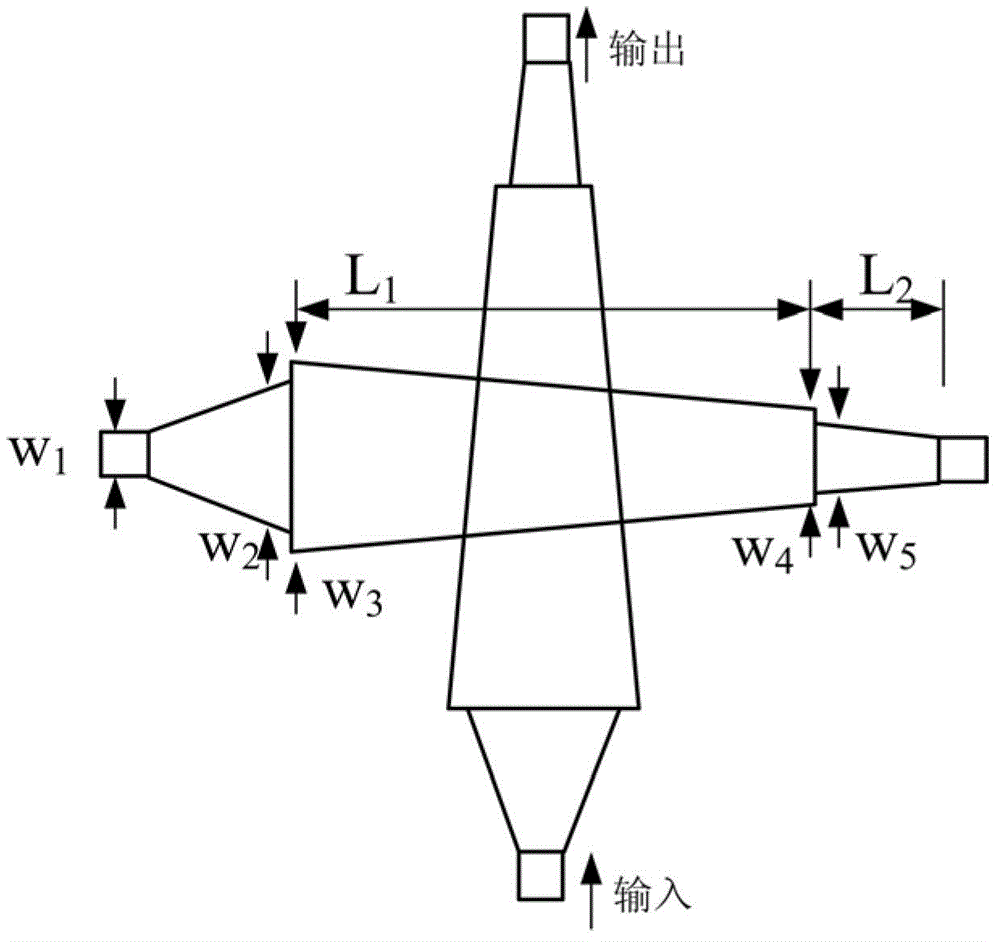
[0015] refer to Figure 1~Figure 4 , a criss-cross waveguide based on the principle of linear tapered multimode interference consists of two identical parts. One of the sections consists of a straight waveguide region, a tapered waveguide region, a tapered multimode interference region, a tapered waveguide region and a straight waveguide region. The two parts intersect vertically, and the intersecting area is in the cone-shaped multimode interference area.

[0016] All domain modules are based on SOI materials with silicon and silicon dioxide having refractive indices of 3.48 and 1.46, respectively. The refractive index difference between the waveguide core and the cladding is 2.02. Since the refractive index difference between the waveguide core and the cladding is large, it is beneficial to confine the light in the core. The size of the waveguide can be made very small, which ...


PUM


Abstract

The invention discloses a cross waveguide based on a linear tapered multimode interference principle. The cross waveguide comprises a vertical portion and a horizontal portion, each of the vertical portion and the horizontal portion is composed of a front straight waveguide area, a front tapered waveguide area, a tapered multimode interference area, a rear tapered waveguide area and a rear straight waveguide area which are sequentially connected, the horizontal portion and the vertical portion are perpendicularly crossed, and a crossed area is located in the tapered multimode interference area. The cross waveguide based on the linear tapered multimode interference principle has the advantage of being low in loss and crosstalk and small in size.

Description

technical field [0001] The invention belongs to the technical field of optical communication, and is especially used in optical devices with a cross waveguide structure, such as a micro-ring resonant filter and a micro-ring resonant wavelength division multiplexer with a cross waveguide structure. technical background [0002] Silicon-based nanowaveguide is one of the important materials for manufacturing integrated optical communication devices. The refractive index difference between the core and cladding of the waveguide is very large, so it is beneficial to confine light in the core. The size of the waveguide can be made very small. It is more suitable for the requirements of high-density integration of large-scale integrated optical circuits. And because of the silicon-based waveguide, it is compatible with the current standard CMOS process. Optical waveguides are fundamental photonic interconnect devices. For sub-micron-scale silicon-based nanowaveguides, the transmi...

Claims


Application Information

Patent Timeline
IPC IPC(8): G02B6/10G02B6/122
Inventor 乐孜纯李锐董文
Owner ZHEJIANG UNIV OF TECH
Why Eureka
Try Eureka