A kind of soi three-strain plane bicmos integrated device and its preparation method

An integrated device, three-strain technology, applied in semiconductor/solid-state device manufacturing, electric solid-state devices, semiconductor devices, etc., can solve problems such as low mobility and limitation of Si material carrier materials

Inactive Publication Date: 2016-01-20
XIDIAN UNIV
View PDF2 Cites 0 Cited by
  • Summary
  • Abstract
  • Description
  • Claims
  • Application Information

AI Technical Summary

Problems solved by technology

[0008] Due to the low mobility of Si materials, the performance of integrated circuits manufactured by SiBiCMOS technology, especially the frequency performance, is greatly limited; for SiGeBiCMOS technology, although SiGeHBT devices are used for bipolar transistors, but for Unipolar devices that restrict the improvement of the frequency characteristics of BiCMOS integrated circuits still use SiCMOS, so these limit the further improvement of the performance of BiCMOS integrated circuits

Method used


Image

  • A kind of soi three-strain plane bicmos integrated device and its preparation method

Examples


Embodiment 1

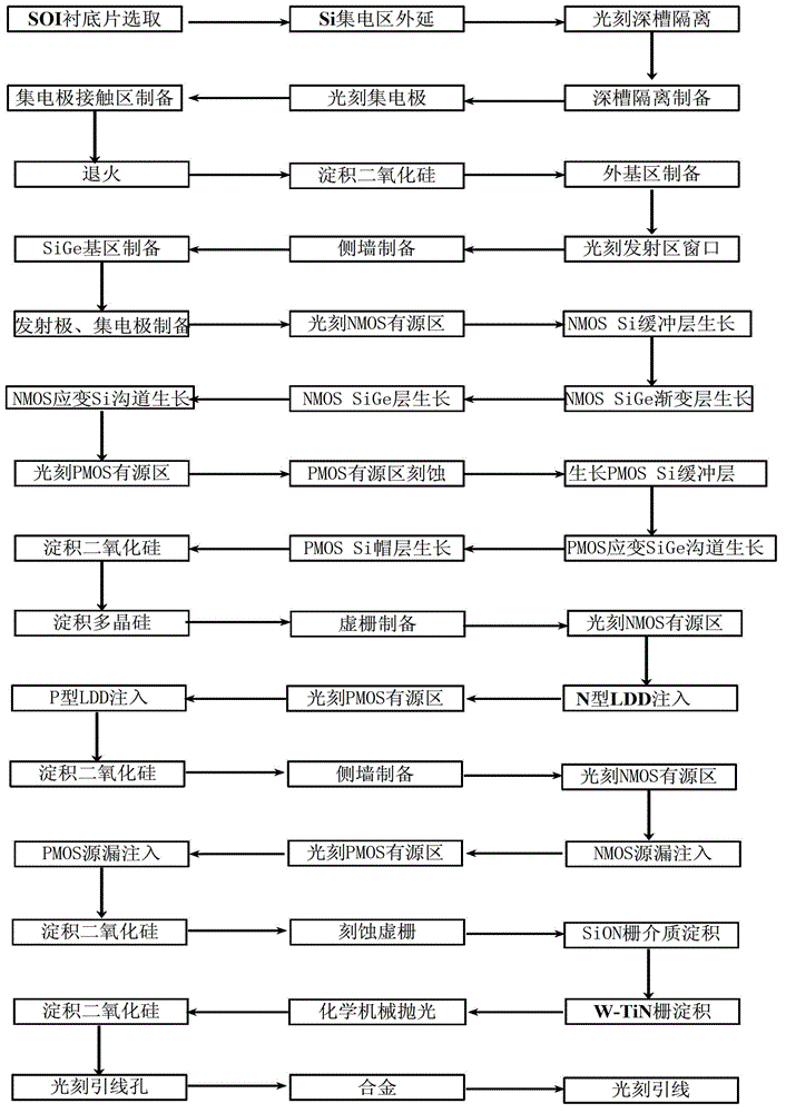
[0119] Embodiment 1: The SOI triple-strained plane BiCMOS integrated device and circuit with a channel length of 22nm are prepared, and the specific steps are as follows:

[0120] Step 1, epitaxial growth.

[0121] (1a) Select the SOI substrate, the support material of the lower layer of the substrate is Si, and the middle layer is SiO 2 , with a thickness of 150nm, and the upper material is doped with a concentration of 1×10 16 cm -3 N-type Si with a thickness of 100nm;

[0122] (1b) Using the chemical vapor deposition (CVD) method, at 600 ° C, grow a layer of N-type epitaxial Si layer with a thickness of 50 nm on the upper Si material, as the collector region, and the doping concentration of this layer is 1× 10 16 cm -3 .

[0123] Step 2, deep trench isolation preparation.

[0124] (2a) Deposit a layer of SiO on the surface of the substrate at 600°C by chemical vapor deposition (CVD) 2 ;

[0125] (2b) In the photolithographic isolation area, a deep groove with a dep...

Embodiment 2

[0184] Embodiment 2: The SOI triple-strained plane BiCMOS integrated device and circuit with a channel length of 30nm are prepared, and the specific steps are as follows:

[0185] Step 1, epitaxial growth.

[0186] (1a) Select the SOI substrate, the support material of the lower layer of the substrate is Si, and the middle layer is SiO 2 , with a thickness of 300nm, and the upper material is doped with a concentration of 5×10 16 cm -3 N-type Si with a thickness of 120nm;

[0187] (1b) Using chemical vapor deposition (CVD), grow an N-type epitaxial Si layer with a thickness of 80nm on the upper Si material at 700°C as the collector region, and the doping concentration of this layer is 5× 10 16 cm -3 .

[0188] Step 2, deep trench isolation preparation.

[0189] (2a) Deposit a layer of SiO on the surface of the substrate at 700°C by chemical vapor deposition (CVD) 2 ;

[0190] (2b) In the photolithographic isolation area, a deep groove with a depth of 3 μm is etched in ...

Embodiment 3

[0249] Embodiment 3: The SOI triple-strained plane BiCMOS integrated device and circuit with a channel length of 45nm are prepared, and the specific steps are as follows:

[0250] Step 1, epitaxial growth.

[0251] (1a) Select the SOI substrate, the support material of the lower layer of the substrate is Si, and the middle layer is SiO 2 , with a thickness of 400nm, and the upper material is doped with a concentration of 1×10 17 cm -3 N-type Si with a thickness of 150nm;

[0252] (1b) Using the method of chemical vapor deposition (CVD), grow a layer of N-type epitaxial Si layer with a thickness of 100nm on the upper layer of Si material at 750°C, as the collector region, and the doping concentration of this layer is 1× 10 17 cm -3 .

[0253] Step 2, deep trench isolation preparation.

[0254] (2a) Deposit a layer of SiO on the surface of the substrate at 800°C by chemical vapor deposition (CVD) 2 ;

[0255] (2b) In the photolithographic isolation area, a deep groove w...


PUM

PropertyMeasurementUnit
thicknessaaaaaaaaaa
thicknessaaaaaaaaaa
thicknessaaaaaaaaaa

Abstract

The invention discloses an SOI (silicon-on-insulator) three-strain planar BiCMOS (complementary metal oxide semiconductor) integrated device and a preparation method thereof. The method includes: growing an N-type Si epitaxial layer on an SOI substrate to serve as a collector region of a bipolar device, preparing deep grooves for isolation, and sequentially preparing base polycrystals, a base region, an emitter region and a collector to form an SiGe HBT (heterojunction bipolar transistor) device; photoetching grooves in an active region of an NMOS device, growing materials of four layers in the grooves, and preparing a gate dielectric layer and gate polycrystals in the active region of the NMOS device to form the NMOS device; photoetching grooves in an active region of a PMOS device, growing materials of five layers in the grooves, and preparing a drain and a grid on the active region of the PMOS device to form the PMOS device; and photoetching leads to form the SOI three-strain planar BiCMOS integrated device and circuits. The emitter, the base and the collector of the SiGe HBT device are all polycrystals which can be partially made on an oxide layer to reduce the active region area of the device, and accordingly the size of the device is reduced, the integration level of the circuits is increased, and performances of the SOI three-strain planar BiCMOS integrated circuits are enhanced.

Description

technical field [0001] The invention belongs to the technical field of semiconductor integrated circuits, and in particular relates to an SOI three-strain plane BiCMOS integrated device and a preparation method. Background technique [0002] The integrated circuit, which appeared in 1958, is one of the most influential inventions of the 20th century. Microelectronics, which was born based on this invention, has become the basis of existing modern technology and is accelerating the process of knowledge and informationization of human society. At the same time It also changed the way people think. It not only provides humans with a powerful tool to transform nature, but also opens up a broad space for development. [0003] Semiconductor integrated circuits have become the basis of the electronics industry, and people's huge demand for the electronics industry has prompted the rapid development of this field. In the past few decades, the rapid development of the electronics i...

Claims


Application Information

Patent Timeline
Patent Type & Authority Patents(China)
IPC IPC(8): H01L27/12H01L21/84
Inventor 王斌宣荣喜张鹤鸣胡辉勇宋建军舒斌李妤晨郝跃
Owner XIDIAN UNIV
Why Eureka
Try Eureka