Semiconductor packaging method for forming two-sided electromagnetic shielding layer as well as construction thereof

A technology of electromagnetic shielding layer and packaging method, which is applied in semiconductor/solid-state device manufacturing, semiconductor device, semiconductor/solid-state device components and other directions, can solve the problems of insufficient carrying capacity of substrate mother sheet 110, plated through hole 117 covering connection, etc., To achieve the effect of the best side electromagnetic shielding effect

Inactive Publication Date: 2012-10-31
POWERTECH TECHNOLOGY
View PDF5 Cites 26 Cited by
  • Summary
  • Abstract
  • Description
  • Claims
  • Application Information

AI Technical Summary

Problems solved by technology

Before forming the electromagnetic shielding layer 152, a half-cut step must be performed, which cuts through the sealant 130 from above along the cutting line 114 until removing a part of the plated through holes 117, and the half-cut groove 140 formed The depth exceeds the thickness of the sealing body 130, which is about two-thirds of the overall thickness, and a part of the mother substrate 110 is also cut off, resulting in insufficient carrying capacity of the mother substrate 110
In addition, the thickness of the base substrate 110 should be increased, approximately greater than the thickness of the encapsulant 130, so as to provide sufficient half-cut exposed areas of the plated through holes 117, otherwise the plated through holes 117 may not be successfully shielded electromagnetically. Layer 152 Covering Connections
Therefore, the existing electromagnetic shielding layer 152 is a single-sided covering type, and the mother substrate must be designed with a special ground connection structure and must have a thickness that can provide sufficient support strength after half-cutting

Method used


Image

  • Semiconductor packaging method for forming two-sided electromagnetic shielding layer as well as construction thereof
  • Semiconductor packaging method for forming two-sided electromagnetic shielding layer as well as construction thereof
  • Semiconductor packaging method for forming two-sided electromagnetic shielding layer as well as construction thereof

Examples


no. 1 Embodiment

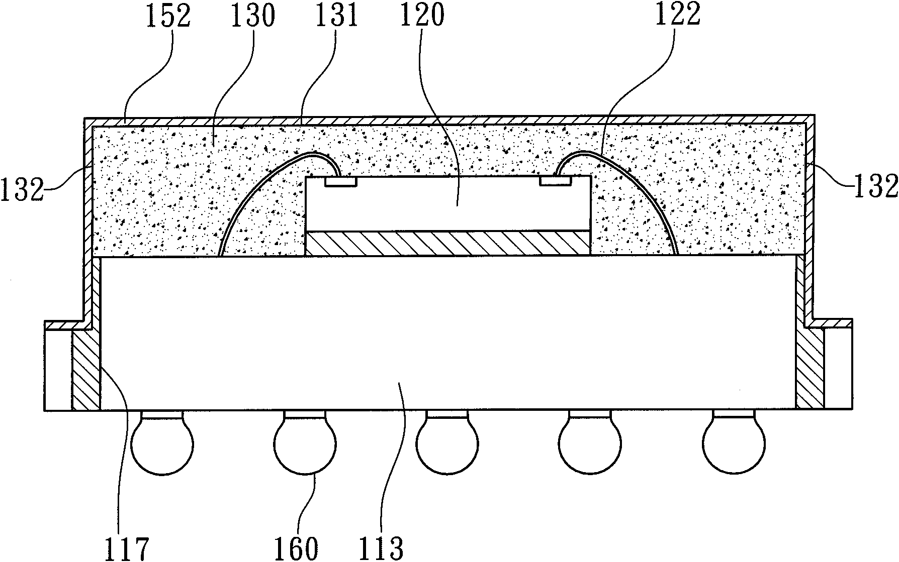
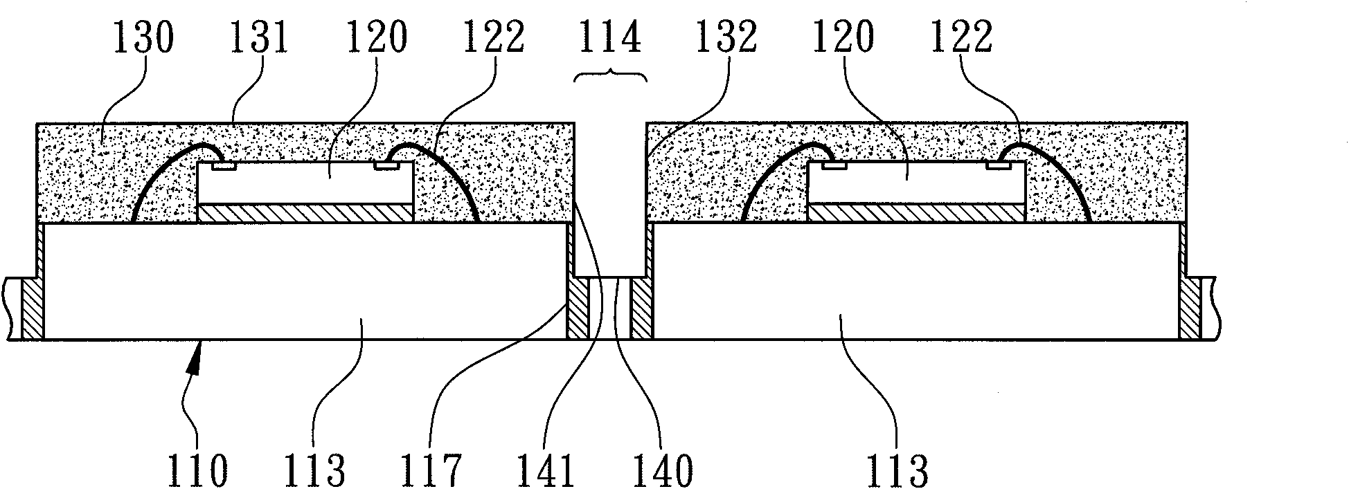
[0057] According to the first embodiment of the present invention, a semiconductor packaging method and structure for forming a double-sided electromagnetic shielding layer are illustrated in Figure 3A to Figure 3I A schematic cross-sectional view of each step to form an element, and a detailed description of each step is as follows.

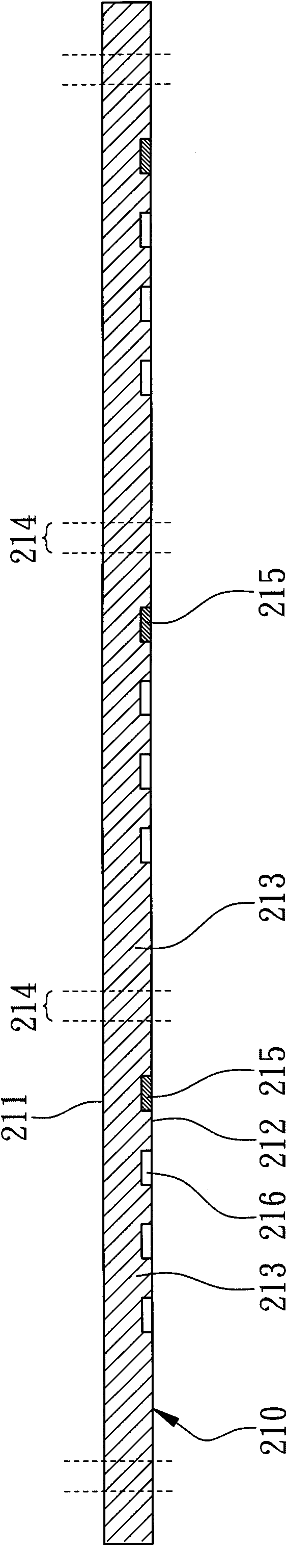
[0058] First, if Figure 3A and Figure 4 As shown, a mother substrate 210 is provided, and the mother substrate 210 has an upper surface 211 and a lower surface 212 . The base substrate 210 can be a strip-shaped printed circuit board or a strip-shaped flexible circuit board, with a single-layer or multi-layer circuit structure inside. The upper surface 211 is used for chip placement, and the lower surface 212 is a surface to be bonded to the outer surface of the semiconductor package structure. The lower surface 212 can be provided with a plurality of external pads 216 arranged in a matrix. The substrate master 210 includes a plurality of ...


PUM


Abstract

The invention discloses a semiconductor packaging method for forming a two-sided electromagnetic shielding layer, which is characterized in that a baseplate does not require a special grounding structure, or scribe line plated-through-holes are not required to be thickened, and grounding connection of the electromagnetic shielding layers is manufactured easily. Firstly, a baseplate master slice is provided, and alignment marks for grounding connection are arranged at the corners of baseplate units. After the steps of die bonding and die molding, multiple semi-cut slots are formed in the lower surface of the baseplate master slice and along the scribe lines, and penetrate the baseplate master slice. A first electromagnetic shielding layer is patterned and formed on the lower surface of the baseplate master slice, covers and is connected to the alignment marks, and is further formed in the semi-cut slots. After monomerization cutting of die molding bodies, a second electromagnetic shielding layer is formed on the top surfaces and the cut side surfaces of the die molding bodies, and is further connected to the first electromagnetic shielding layer.

Description

technical field [0001] The present invention relates to the packaging technology of semiconductor devices, in particular to a semiconductor packaging method and structure for forming double-sided electromagnetic shielding layers. Background technique [0002] A semiconductor chip is a tiny electronic component. Even after being packaged, it may still be subject to electromagnetic interference (EMI), which may cause chip operation abnormality or electrical function failure. Especially, the higher the operation frequency of the chip, the more susceptible it is to interference. Therefore, according to one of the known conventional methods, an electromagnetic shielding layer (or a radio frequency shielding layer) is covered on the outer surface of the encapsulant in which the chips are sealed. However, the electromagnetic shield must be effectively connected to ground in order to exert a good shielding effect. In addition, the encapsulant itself is an electrical insulating mate...

Claims


Application Information

Patent Timeline
Patent Type & Authority Applications(China)
IPC IPC(8): H01L21/56H01L23/552H01L23/31
CPCH01L24/97H01L2924/15311H01L2224/97H01L2924/15159H01L2224/73265H01L2224/48227H01L2224/32225H01L21/561H01L2924/3025H01L23/552H01L24/73H01L2224/04042H01L2224/06136H01L2924/181H01L2924/1815H01L2924/00012H01L2224/85H01L2924/00
Inventor 徐守谦
Owner POWERTECH TECHNOLOGY
Why Eureka
Try Eureka