FPGA (Field Programmable Gate Array) timing driven layout method with timing constraints

A technology of timing constraints and layout methods, applied in the field of electronics

Active Publication Date: 2012-11-07
FUDAN UNIV
View PDF5 Cites 27 Cited by
  • Summary
  • Abstract
  • Description
  • Claims
  • Application Information

AI Technical Summary

Problems solved by technology

However, as the scale of the FPGA array continues to expand, the complexity of circuit design continues to increase, and designers have higher and higher requirements for the flexibility of FPGA timing-driven algorithms. In the past, FPGA timing optimized only for clock cycles Driven layout algorithms are difficult to meet these requirements of today's designers

Method used


Image

  • FPGA (Field Programmable Gate Array) timing driven layout method with timing constraints
  • FPGA (Field Programmable Gate Array) timing driven layout method with timing constraints
  • FPGA (Field Programmable Gate Array) timing driven layout method with timing constraints

Examples


Embodiment Construction

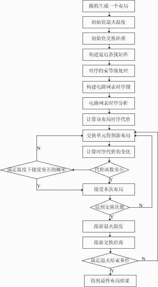
[0050] The method of the present invention is specifically described below through a simulation test example: adding minimum clock cycle constraints and input and output delay constraints at the same time.

[0051] (1) Constraint equivalence of the minimum clock period. Timing analysis, find out all the timing paths in the input netlist, and count the delay value of each timing path.

[0052] (2) Equivalent input and output delay constraints. Add the values ​​of the input and output delay constraints to the corresponding timing analysis paths. For the timing path specified by the input delay constraint, the starting point value of the timing path T init Change from the original 0 to the input constraint value C1. Similarly, for the path specified by the output delay constraint, the end point value of the timing path is changed from the original T arrival change to T arrival +C2, C2 is the output delay constraint value of the timing path.

[0053] (3) Perform timing anal...


PUM


Abstract

The invention belongs to the technical field of electronics, specifically, discloses an FPGA (Field Programmable Gate Array) timing driven layout method with timing constraints. According to the layout method provided by the invention, four types of timing constraints are proposed as follows: a clock period constraint, an input output delay constraint, a specific timing path constraint and a wire network maximum delay constraint. The main idea for processing the four types of timing constraints is to add the information of the timing constraints into a timing analysis step to process the timing constraints as a part of a final cost function. The method provided by the invention can process the timing constraints set by the users, so that the flexibility of an FPGA timing layout algorithm is increased greatly, and simultaneously, the correctness of the layout algorithm also can be guaranteed.

Description

technical field [0001] The invention belongs to the field of electronic technology, and in particular relates to an FPGA timing-driven layout method with timing constraints. Background technique [0002] When the traditional FPGA layout method optimizes the timing performance of the circuit, the timing-driven algorithm adopted only processes the minimum clock cycle of the circuit to obtain the highest frequency. However, as the scale of the FPGA array continues to expand, the complexity of circuit design continues to increase, and designers have higher and higher requirements for the flexibility of FPGA timing-driven algorithms. In the past, FPGA timing optimized only for clock cycles Driven layout algorithms are difficult to meet these requirements of today's designers. Therefore, it is necessary to propose a new FPGA timing-driven placement method to meet various timing constraints proposed by designers. Contents of the invention [0003] The purpose of the present inv...

Claims


Application Information

Patent Timeline
Patent Type & Authority Applications(China)
IPC IPC(8): G05B19/05
Inventor 来金梅李华冈王元王键王臻
Owner FUDAN UNIV
Why Eureka
Try Eureka