
Memory device with external chip controller and manufacturing method of memory device

A manufacturing method and memory technology, applied in the direction of static memory, digital memory information, semiconductor/solid-state device manufacturing, etc., can solve the problems of increased process cost and expensive production line

Active Publication Date: 2012-11-07
MACRONIX INT CO LTD
View PDF7 Cites 6 Cited by
  • Summary
  • Abstract
  • Description
  • Claims
  • Application Information

AI Technical Summary

Problems solved by technology

Since both the memory array and the peripheral circuitry require support for the manufacturing steps, the production line used to implement the memory device may be expensive or compromised by the circuitry required to manufacture the peripheral circuitry
This will lead to the use of higher-end technology to manufacture integrated circuits for memory devices, resulting in higher process costs

Method used


Image

  • Memory device with external chip controller and manufacturing method of memory device
  • Memory device with external chip controller and manufacturing method of memory device
  • Memory device with external chip controller and manufacturing method of memory device

Examples


Embodiment Construction

[0040] Embodiments of the invention will cooperate with the illustrated Figure 1 to Figure 10 For details in the following.

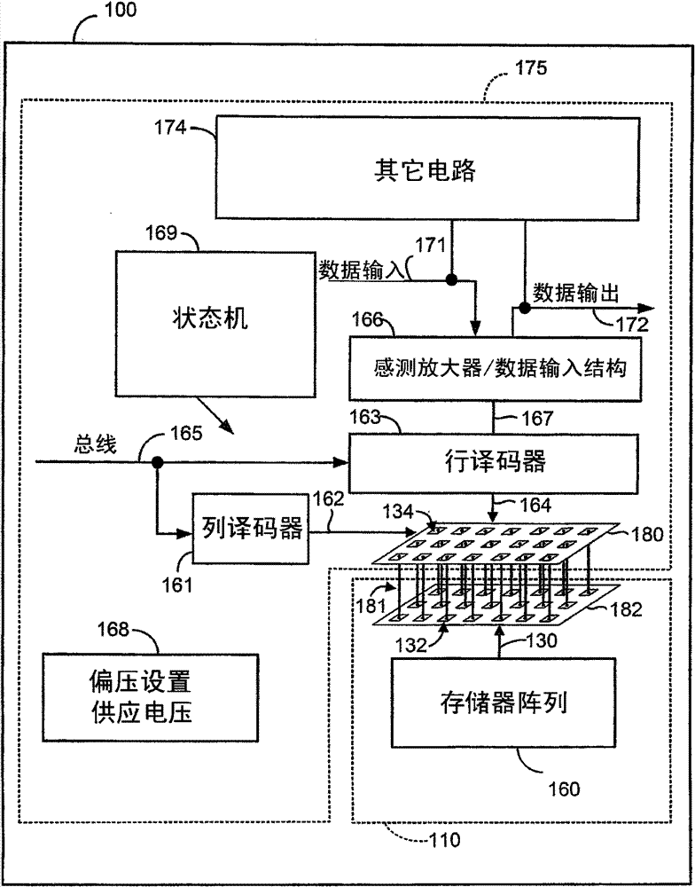
[0041] figure 1 A block diagram of a simplified integrated circuit memory device 100 is shown. The integrated circuit memory device 100 includes a memory circuit 100 and a peripheral circuit 175. The memory circuit and the peripheral circuit described here are physically separated from the device 100. on different layers, and are connected to each other through an interconnection interface 181 . The term “joined” or “joining” used herein means that the memory circuit 110 is attached, fixed, or otherwise physically connected to the peripheral circuit 175 . This term covers that the memory circuit 110 is directly attached to the peripheral circuit 175, such as through bonding. The term also covers that the memory circuit 110 is configured to be indirectly connected to the peripheral circuit 175 through an interposer unit or element between the memory ...


PUM


Abstract

The invention discloses an integrated circuit memory device and a manufacturing method thereof. The method and the device are applicable to low-cost processes, and the device comprises a memory circuit and a peripheral circuit. The memory circuit and the peripheral circuit of the device are positioned on different layers achieved in a laminated structure. A memory circuit layer and a peripheral circuit layer comprise complementary interconnection surfaces, and electrical interconnection can be established by the aid of matching of the complementary interconnection surfaces of the memory circuit and the peripheral circuit. Besides, the memory circuit layer and the peripheral circuit layer can be formed on different substrates respectively on different production lines by means of different processes. By the manufacturing means, the memory circuit layer and the peripheral circuit layer can be manufactured by using independent process equipment and technologies respectively, one process technology is used for manufacturing memory arrays, and the other process technology is used for manufacturing peripheral circuits. Further, the independent circuits can be laminated and bonded together.

Description

technical field [0001] The invention relates to an integrated circuit memory device and a manufacturing method thereof. Background technique [0002] When manufacturing high-density memory devices, the data storage capacity per unit area on the integrated circuit will be a key indicator. Therefore, when the critical dimension technology of the memory device has reached the bottleneck, in order to achieve a higher storage density per bit and reduce the production cost per bit, it is generally recommended to stack multiple levels of memory cells. In addition, new memory technologies are being developed, including phase change memory, ferromagnetic memory, and metal oxide based memory. [0003] Memory technology requires a series of different process steps, followed by the fabrication of minor peripheral circuits such as address decoders, state machines, and command decoders. Since both the memory array and the peripheral circuitry require manufacturing steps to support it, t...

Claims


Application Information

Patent Timeline
IPC IPC(8): H01L21/98H01L21/768H01L25/065G11C11/34
Inventor 陈士弘吕函庭谢光宇
Owner MACRONIX INT CO LTD
Features
  • Generate Ideas
  • Intellectual Property
  • Life Sciences
  • Materials
  • Tech Scout
  • Unparalleled Data Quality
  • Higher Quality Content
  • 60% Fewer Hallucinations
Learn More