Apparatus for bonding semiconductor chip

A semiconductor and chip technology, applied in the field of semiconductor chip bonding equipment, can solve the problems of not effectively controlling the substrate drive unit, and achieve the effects of reducing estimated costs, increasing response speed, and eliminating installation errors

Inactive Publication Date: 2012-11-07
IPS SYST
View PDF3 Cites 1 Cited by
  • Summary
  • Abstract
  • Description
  • Claims
  • Application Information

AI Technical Summary

Problems solved by technology

Although a general semiconductor package requires a positional accuracy of about 10 μm, a semiconductor package with increased integration requires a higher positional accuracy of about 5 μm
[0009] This conventional semiconductor chip bonding apparatus has the following problems: the substrate driving unit for transferring or rotating the printed circuit board is not effectively controlled when the semiconductor chip is mounted on the printed circuit board, and thus the gap between the semiconductor chip and the printed circuit board The assembly error exceeds the allowable error of semiconductor packages with high integration

Method used


Image

  • Apparatus for bonding semiconductor chip
  • Apparatus for bonding semiconductor chip
  • Apparatus for bonding semiconductor chip

Examples


Embodiment Construction

[0024] Hereinafter, exemplary embodiments of a semiconductor chip bonding apparatus according to the present invention will be described with reference to the accompanying drawings.

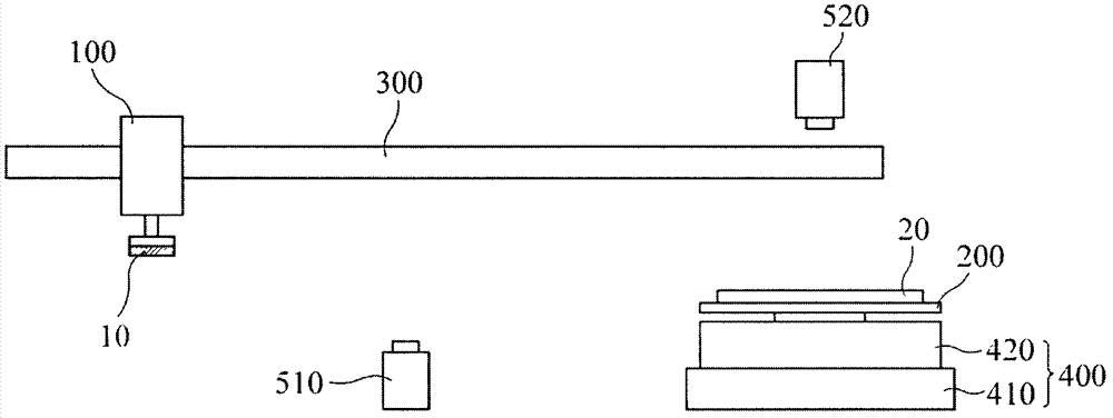
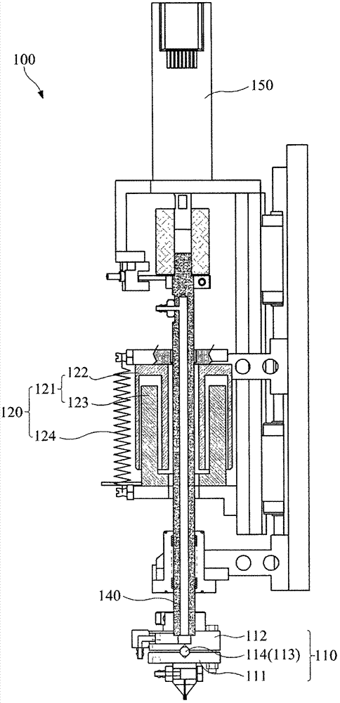
[0025] figure 2 is a view schematically illustrating a semiconductor chip bonding apparatus according to an exemplary embodiment of the present invention; image 3 for figure 2 A cross-sectional view of a chip adsorption unit in a semiconductor chip bonding apparatus of ; Figure 4 and Figure 5 for illustration figure 2 A view of how the semiconductor die bonding equipment operates; Figure 6 to explain figure 2 A view of the uses of the first driver and the second driver in the semiconductor die bonding apparatus of ; and Figure 7 for illustration figure 2 A view of how a tilt adjuster in a semiconductor die bonding equipment operates.

[0026] refer to Figure 2 to Figure 7 , the semiconductor chip bonding apparatus according to this exemplary embodiment is to minimize a mountin...


PUM


Abstract

An apparatus for bonding a semiconductor chip. A chip adsorption unit adsorbs the semiconductor chip at an initial position and releases the adsorption of the semiconductor chip at a mounting position at which the semiconductor chip is mounted on a printed circuit board. A board supporting plate is arranged to be separated from the initial position of the chip adsorption unit. The board supporting plate supports the printed circuit board. A chip transfer unit transfers the chip adsorption unit. A board driving unit transfers or rotates the board supporting plate.

Description

technical field [0001] The present invention relates to a semiconductor chip bonding apparatus, and more particularly, to a semiconductor chip bonding apparatus in which a semiconductor chip can be more accurately aligned and mounted on a printed circuit board. Background technique [0002] In order to actually use a semiconductor device manufactured on a wafer, the semiconductor device must be cut from the wafer into chip units and manufactured into a package. The semiconductor package not only mechanically supports and fixes the semiconductor chip and protects the semiconductor chip from the outside, but also provides an electrical connection path and a heat discharge path to the semiconductor chip. [0003] In the early days, semiconductor packages commonly used lead frames as package substrates for mechanically and electrically connecting semiconductor chips and external systems. However, as the number of input / output pins increases and the operation speed increases, th...

Claims


Application Information

Patent Timeline
Patent Type & Authority Applications(China)
IPC IPC(8): H05K3/30
CPCH01L2224/16225H01L2224/75H01L2224/81H01L24/81H05K13/0061H05K13/046H05K13/0409
Inventor 李寿镇
Owner IPS SYST
Why Eureka
Try Eureka