Electronic device housing and manufacturing method therefor

A manufacturing method and technology of electronic equipment, applied in the direction of casing/cabinet/drawer components, antenna support/installation device, structural form of radiation unit, etc. Antenna signal reception and other issues, to achieve the effect of diverse colors, soft and smooth hand feeling, and strong tear resistance

Active Publication Date: 2012-11-14
LOVEPAC CONVERTING BEIJING +1
View PDF5 Cites 27 Cited by
  • Summary
  • Abstract
  • Description
  • Claims
  • Application Information

AI Technical Summary

Problems solved by technology

Protecting the antenna with a protective cover will obviously increase the thickness of the mobile phone case, which will affect the appearance, and the protective cover is also easy to fall off, not firm, and if the thickness is too large, it will even affect the signal reception of the antenna
When spraying protective paint, the protective paint cannot be sprayed too thick at one time, and it is easy to fall off if it is too thick; too thin is not wear-resistant, and it is difficult to cover the antenna metal layer protruding from the surface of the shell
If you spray paint multiple times, you have to spray it again and polish it once. The process is complicated and the cost is high

Method used


Image

  • Electronic device housing and manufacturing method therefor
  • Electronic device housing and manufacturing method therefor

Examples


Embodiment Construction

[0025] In order to have a clearer understanding of the technical features, purposes and effects of the present invention, the specific implementation manners of the present invention will now be described with reference to the accompanying drawings. Wherein, the same parts adopt the same reference numerals.

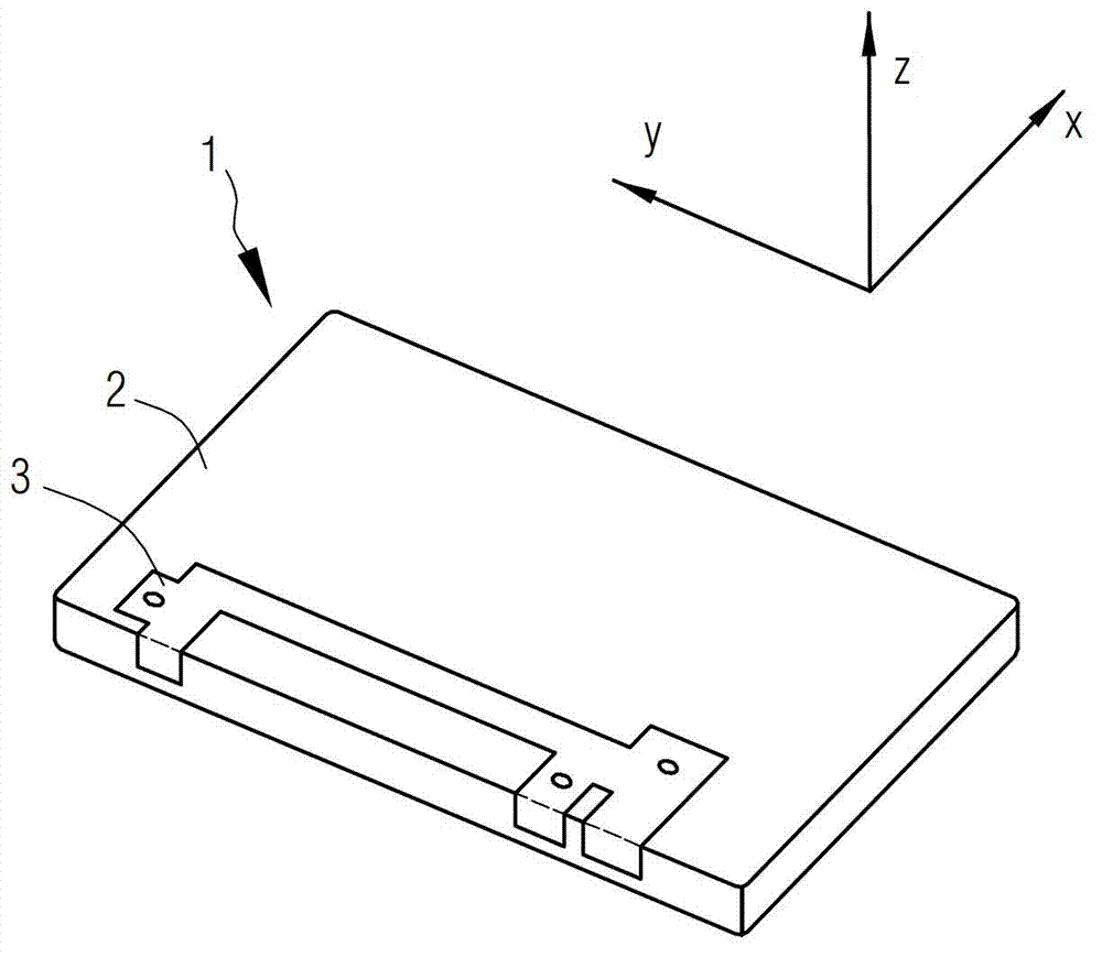
[0026] Taking the back cover of a mobile phone case as an example, the structure and manufacturing method of the electronic device case according to the present invention will be described in detail below. Of course, those skilled in the art should understand that the electronic device housing of the present invention is not limited to mobile phone electronic devices, but can also be widely used in various electronic devices with wireless communication functions, such as mobile phones, computers, and tablet computers. Wait.

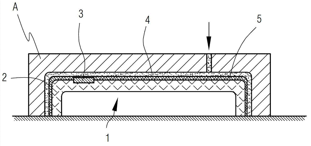
[0027] figure 1 Shown is a structural schematic diagram of forming a metal antenna on the surface of an electronic device casing by LDS technology...


PUM


Abstract

The invention discloses an electronic device housing and a manufacturing method for the electronic device housing. The manufacturing method comprises the following steps: forming a metal antenna on the surface of an active plastic layer of the electronic device housing by an LDS (Laser Direct Structuring) technology; spraying a layer of bottom coating agent on the surface of the active plastic layer and the surface of the metal antenna; moulding a layer of liquid silica gel on the surface of the active plastic layer sprayed with the bottom coating agent and the surface of the metal antenna in an injection way, drying the liquid social gel to form a silica gel protective layer. According to the electronic device housing and the manufacturing method for the electronic device housing, the silica gel protective layer is moulded on the surface of the electronic device housing in an injection way by liquid silica gel, and can be suitable for various different using environments for the electronic device housing, can be manufactured to be very soft or relatively hard, and has high anti-tearing and anti-stretching strength; simultaneously, the product is diversified in colour, smudginess-resistant, chemical-resistant, and soft and smooth in hand feeling.

Description

technical field [0001] The present invention relates to an electronic equipment housing with a metal antenna formed by LDS technology and a manufacturing method thereof. The electronic device housing can be widely used in various electronic devices with wireless communication functions, such as mobile phones, computers, tablet computers and the like. Background technique [0002] Laser direct structuring (LDS) technology is a technology developed by German LPKF company, which has been widely used in the production process of mobile phone antennas. LDS technology uses a laser to carve antenna circuit traces on the surface of thermoplastic composite components, and activates the organometallic additives in this thermoplastic material by laser, exposing the metal particles in the organic metal additives, such as copper particles, to the components The surface of the circuit trace, and finally the laser-activated part of the component, that is, the surface of the circuit trace,...

Claims


Application Information

Patent Timeline
Patent Type & Authority Applications(China)
IPC IPC(8): H05K5/02H01Q1/40H01Q1/22
Inventor 岳衡
Owner LOVEPAC CONVERTING BEIJING
Why Eureka
Try Eureka