

Liquid crystal display substrate, manufacturing method thereof, liquid crystal panel and display device
A liquid crystal display and liquid crystal panel technology, which is applied in the field of liquid crystal panels and display devices, liquid crystal display substrates and their production, and can solve problems such as unsatisfactory flattening degree, low flattening degree of array substrate surface, and affecting the display quality of liquid crystal panels. , to achieve the effect of improving quality, improving yield rate, and high degree of planarization
- Summary
- Abstract
- Description
- Claims
- Application Information
AI Technical Summary
Problems solved by technology
Method used
Image

Examples
Embodiment Construction
[0037] The following will clearly and completely describe the technical solutions of the embodiments of the present invention with reference to the accompanying drawings in the embodiments of the present invention. Obviously, the described embodiments are only part of the embodiments of the present invention, not all of them. Based on the embodiments of the present invention, all other embodiments obtained by persons of ordinary skill in the art without making creative efforts belong to the protection scope of the present invention.
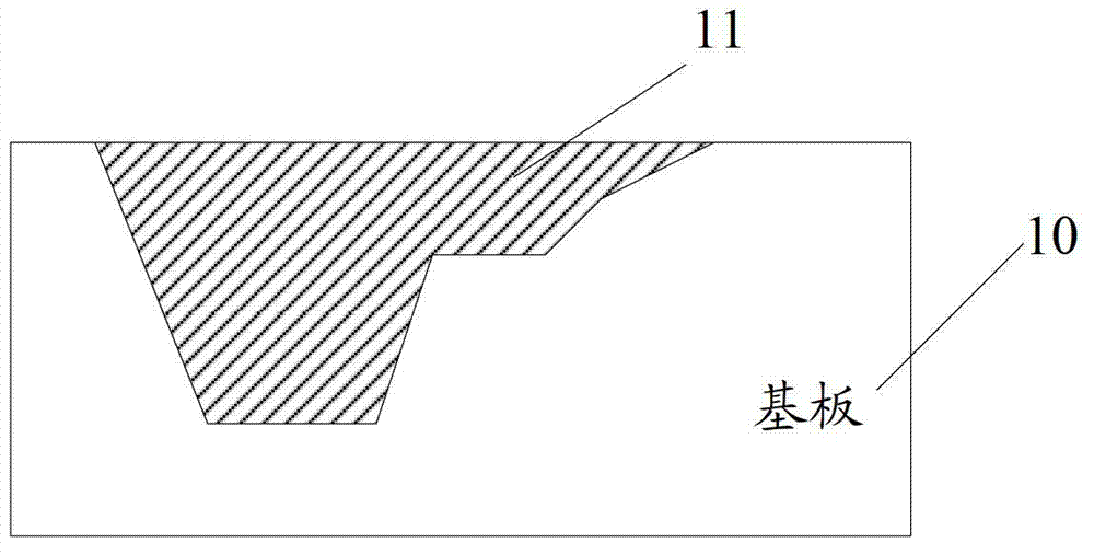
[0038] figure 1 A schematic diagram of a liquid crystal display substrate provided by an embodiment of the present invention. refer to figure 1 An embodiment of the present invention provides a liquid crystal display substrate, the liquid crystal display substrate includes a substrate 10 and a display component (not shown in the figure), and the substrate may be a glass substrate. A groove 11 is provided on the substrate 10 (as shown by the sha...
PUM
 Abstract
Description
Claims
Application Information