PROM circuit framework for FPGA configuration
A circuit and reset circuit technology, applied in the field of PROM circuit architecture, can solve the problems of unfavorable configuration scale expansion, PROM chip storage capacity is small, FLASH memory cannot directly meet the needs of different configuration modes of FPGA, etc.
- Summary
- Abstract
- Description
- Claims
- Application Information
AI Technical Summary
Problems solved by technology
Method used
Image
Examples
Embodiment Construction
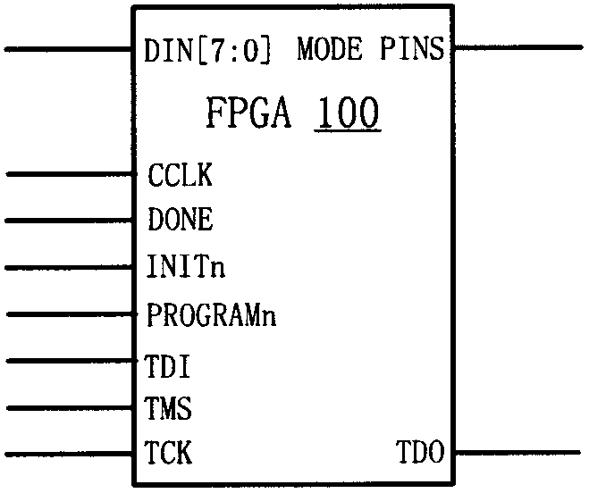
[0084] figure 1 It is a schematic diagram of FPGA 100 device configuration interface, and its configuration-related interface signals mainly include: configuration data input signal DIN[7:0], mode selection pin MODE PINS, FPGA configuration clock signal CCLK, configuration completion signal DONE, configuration initialization signal INITn, a programming enable signal PROGRAMn, a test data input signal TDI, a test mode selection signal TMS, a test clock signal TCK and a test data output signal TDO. Among them, the test data input signal TDI, the test mode selection signal TMS, the test clock signal TCK and the test data output signal TDO are also signals dedicated to the boundary scan circuit in the FPGA device.
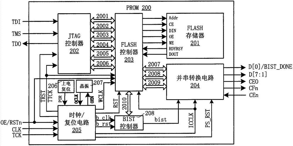
[0085] figure 2 It is a module detailed diagram of the PROM 200 circuit architecture of the present invention, including a FLASH memory 201, a JTAG controller 202, a FLASH controller 203, a parallel-to-serial conversion circuit 204, a clock reset circuit 205, a power...
PUM
 Abstract
Description
Claims
Application Information
 - R&D
- Intellectual Property
- Life Sciences
- Materials
- Tech Scout
- Unparalleled Data Quality
- Higher Quality Content
- 60% Fewer Hallucinations
Browse by: Latest US Patents, China's latest patents, Technical Efficacy Thesaurus, Application Domain, Technology Topic, Popular Technical Reports.
© 2025 PatSnap. All rights reserved.Legal|Privacy policy|Modern Slavery Act Transparency Statement|Sitemap|About US| Contact US: help@patsnap.com


