Ultrathin full-wave rectifier

A full-wave rectification, ultra-thin technology, applied in the field of rectifiers, can solve the problems of poor heat dissipation between material grains, electronic circuit power supply failure, large product volume, etc., to achieve high reliability, improve work efficiency, and compact structure. Effect

Inactive Publication Date: 2012-11-21
广东良得光电科技有限公司
View PDF4 Cites 1 Cited by
  • Summary
  • Abstract
  • Description
  • Claims
  • Application Information

AI Technical Summary

Problems solved by technology

This prior art is a vertical multi-layer structure, although fast encapsulation can be used, but the manufactured product has a large volume, complex process, more raw materials, poor heat dissipation between material grains, and long-term working In this state, it is easy to cause aging, which will cause the power supply failure of the applied electronic circuit

Method used


Image

  • Ultrathin full-wave rectifier
  • Ultrathin full-wave rectifier
  • Ultrathin full-wave rectifier

Examples


Embodiment 1

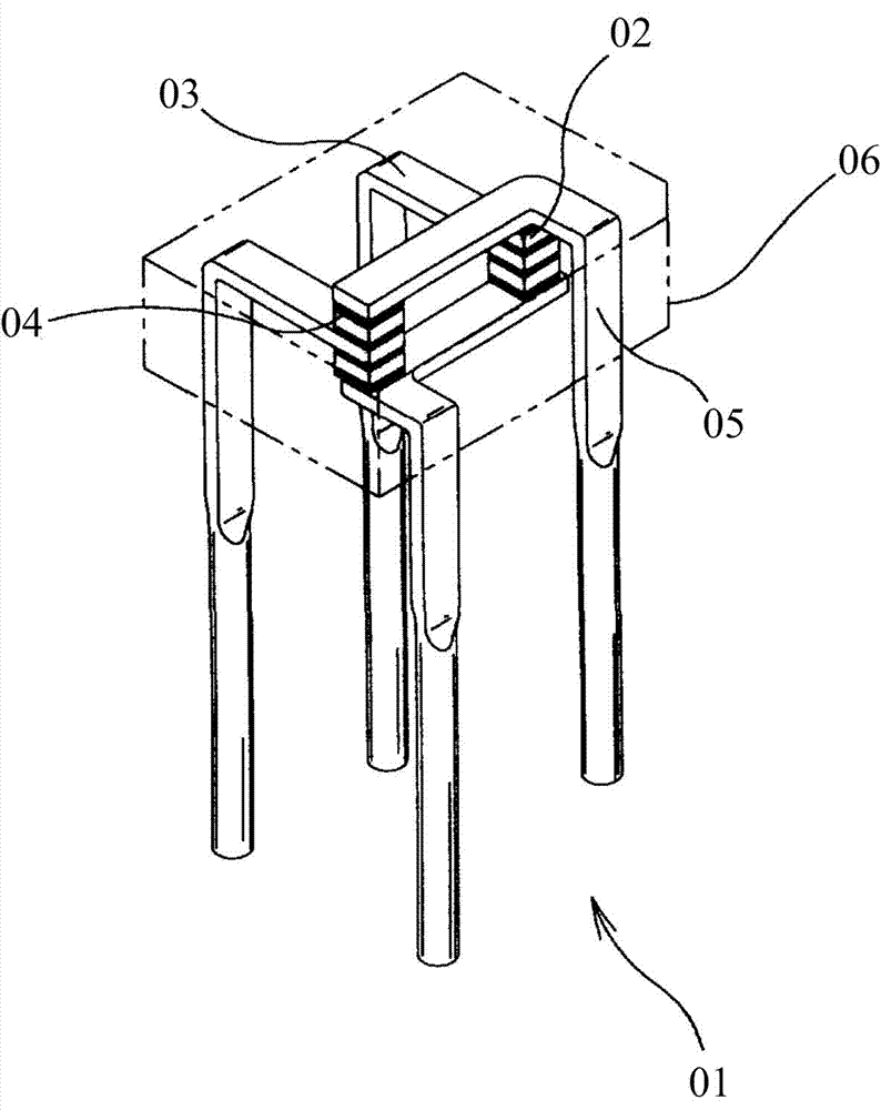
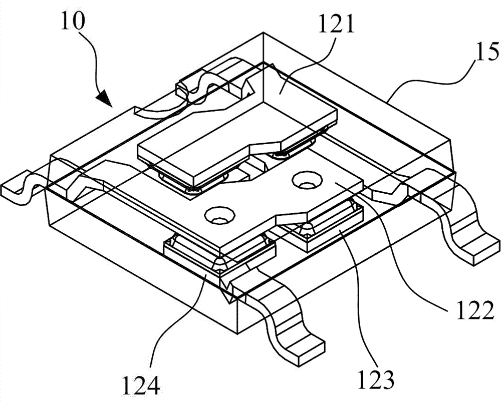
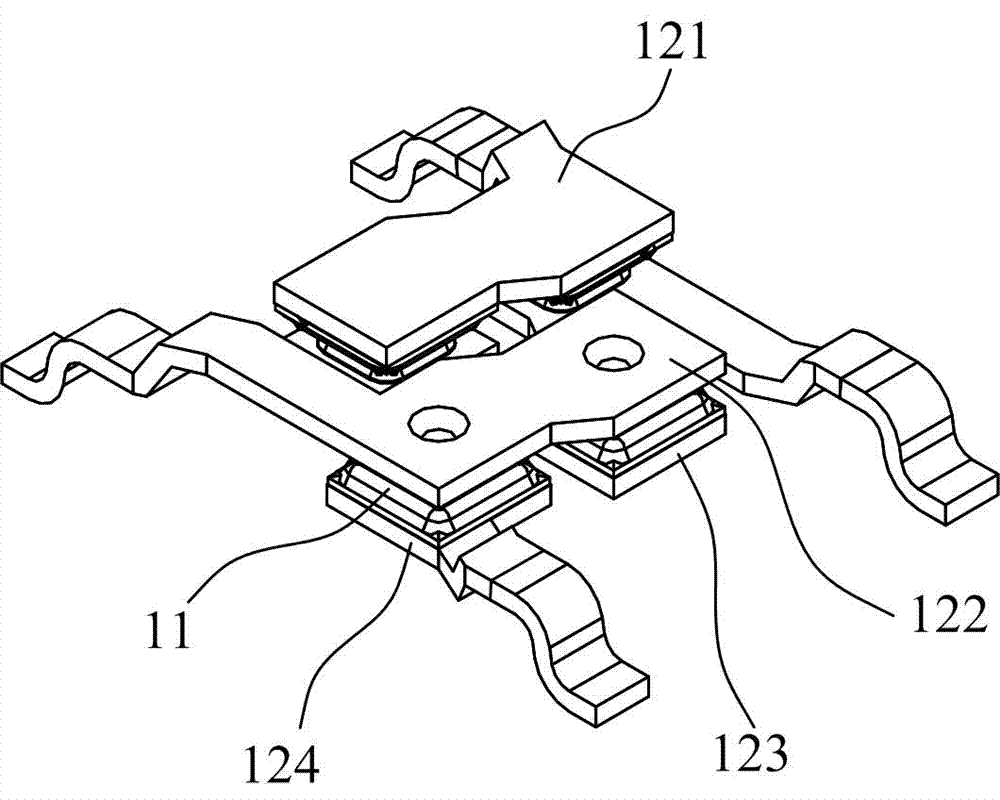
[0030] refer to figure 2 , image 3 , Figure 4 The schematic diagram of the structure of this embodiment is shown.

[0031] In the ultra-thin full-wave rectifier 10 of the embodiment of the present invention, four wafers 11 are included, four electrode contacts 12a, 12b, and the four wafers are arranged in a quadrilateral distribution on a plane, and the polarity of the upper surface of the wafers on each side For reference, the polarity is arranged in order of "different-same-different-same", so that the polarities of the wafers on one pair of sides are the same, and the polarities of the opposite sides are different. In this implementation, it is preferable to arrange the wafers 11 into a parallelogram or a square, and in order to make the structure more compact and reasonable, the present embodiment is preferably a parallelogram distribution, and the parallelogram distribution refers to the formation of a parallelogram distribution on the center line of each wafer, such...

Embodiment 2

[0041] In this embodiment, the FR chip is selected to be assembled into an FR fast rectifier using wafers, so that the reverse recovery time of the ultra-thin full-wave rectifier in this embodiment is between 150 and 1500 nS, and the pitch is set to 2.5 mm, such as Figure 6 The schematic diagram of the structural packaging shown in the figure, other structures are consistent with the description of Embodiment 1, and will not be repeated here.

Embodiment 3

[0043] In this embodiment, the SF chip is selected to be assembled into a SF fast rectifier using wafers, so that the reverse recovery time of the ultra-thin full-wave rectifier in this embodiment is between 15 and 35 nS, and the pitch is set to 4.0 mm. Other structures are the same as The description of Embodiment 1 is consistent, so the description will not be repeated here.


PUM


Abstract

The embodiment of the invention discloses an ultrathin full-wave rectifier which comprises four wafers, four pole contacts and a package glue body, wherein the four wafers are arranged in a quadrilateral shape in a same plane, and polarities of the wafers on adjacent peripheries are in alternating arrangement of different-same in sequence; the pole contacts are divided into an upper-layer group of pole contacts and a lower-layer group of pole contacts; the two pole contacts at the upper layer are respectively used for electrically connecting two wafers with a same polarity on the upper surfaces of the four wafers; the two pole contacts at the lower layer are respectively used for electrically connecting two wafers with different polarities in a same direction on the lower surfaces of the four wafers; and the package glue body is used for packing the wafers and the pole contacts. By adopting the ultrathin full-wave rectifier, a rectifier which is thinner than the conventional rectifier can be produced, and the pin distance between two pins and types of the wafers can be selected according to the actual requirements, so that the ultrathin full-wave rectifier can be applied flexibly, the four wafers are in a plane placing structure, a product can be tightly attached on a radiating surface of a PC (printed circuit) board, relatively good radiating performance can be obtained, the temperature of a PN node can be controlled within a reasonable range, and the working efficiency is improved.

Description

technical field [0001] The invention relates to a rectifier, in particular to an ultra-thin full-wave rectifier. Background technique [0002] At present, the assembly method of the existing bridge rectifiers on the market is vertical assembly, that is, a multi-layer stacked structure in the vertical direction, and the structure is covered with epoxy resin. The packaging method is relatively simple and can be realized on a mold. Sequential packaging has high co-efficiency, but there are also many defects, such as: the positive and negative poles are diagonally positioned, and the volume is large, which is not conducive to the heat dissipation of the internal chip, and is not suitable for highly integrated circuits that require small volume . [0003] The patent announcement number is CN 2369338Y, which discloses a bridge rectifier 01, such as figure 1 As shown, it is packaged in a vertical package, including four chips 02, and every two chips 02 are stacked together, and a...

Claims


Application Information

Patent Timeline
Patent Type & Authority Applications(China)
IPC IPC(8): H01L25/07H01L23/31H01L23/367H02M1/00
CPCH01L24/33H01L2924/181H01L2924/00012
Inventor 苏松得
Owner 广东良得光电科技有限公司
Why Eureka
Try Eureka