Method for manufacturing AlGaInP-LED (Light Emitting Diode) integrated micro display component with single-side electrode structure

A micro-display device and electrode structure technology, applied in the direction of electric solid-state devices, electrical components, semiconductor devices, etc., can solve problems such as difficult fabrication and high substrate thickness requirements, achieve simple structure, avoid physical damage, and improve uniformity of light emission degree of effect

Active Publication Date: 2012-11-21
CHANGCHUN INST OF OPTICS FINE MECHANICS & PHYSICS CHINESE ACAD OF SCI
View PDF5 Cites 10 Cited by
  • Summary
  • Abstract
  • Description
  • Claims
  • Application Information

AI Technical Summary

Problems solved by technology

[0004] The present invention aims to solve the technical problem that the micro-display device in the prior art requires high substrate thickness and is not easy to manufacture in the manufacturing process, and provides a single display device based on AlGaInP light-emitting layer, where the positive and negative electrodes are both located above the substrate. Fabrication method of AlGaInP-LED integrated microdisplay device with surface electrode structure

Method used


Image

  • Method for manufacturing AlGaInP-LED (Light Emitting Diode) integrated micro display component with single-side electrode structure
  • Method for manufacturing AlGaInP-LED (Light Emitting Diode) integrated micro display component with single-side electrode structure
  • Method for manufacturing AlGaInP-LED (Light Emitting Diode) integrated micro display component with single-side electrode structure

Examples


Embodiment Construction

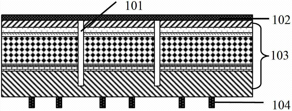
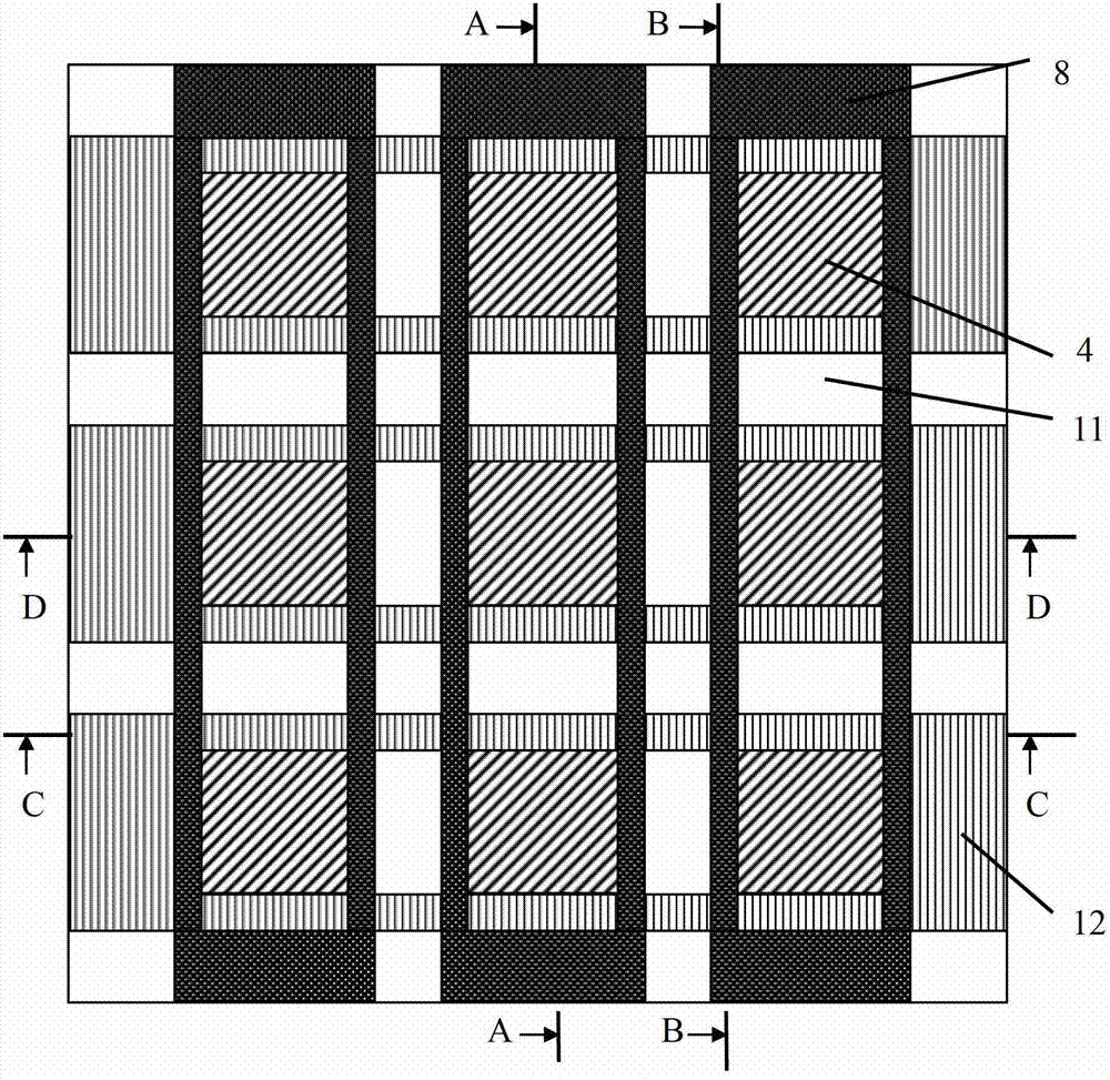
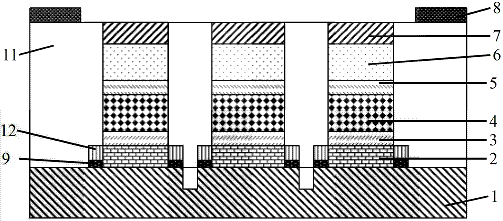
[0033] The inventive concept of the present invention is that for LED array microdisplay devices, the electrode shape is an important factor determining its luminous efficiency and luminous uniformity, and the design of the electrode shape should comprehensively consider the area of ​​the light-transmitting window and the distribution uniformity of the current under the electrode .

[0034] The manufacturing method of the AlGaInP-LED integrated micro-display device with a single-sided electrode structure proposed by the present invention can avoid the technical difficulties caused by separately making electrodes on the front and back. This manufacturing process is not only simple and easy, but also does not cause damage to the device. Therefore, it will not have any impact on the light emission of the device. The device manufactured by the manufacturing process proposed by the present invention has double-striped upper and lower electrodes perpendicular to different planes, wh...


PUM


Abstract

The invention discloses a method for manufacturing an AlGaInP-LED (Light Emitting Diode) integrated micro display component with a single-side electrode structure, wherein the steps comprises: etching multiple first grooves which are mutually intersected on a device body; growing a lower electrode metal layer on the bottom part of each groove to form the lower electrode metal layer; growing an insulating medium layer above a lower electrode; corroding an area of the lower electrode metal layer outside a lower electrode diagram downward till reaching a certain depth in an N-shaped substrate layer in order to form multiple second grooves; filling opaque diaphragms into the second grooves and the upper part of a protection medium of the lower electrode; manufacturing an upper electrode above a light emitting unit; and electroforming upper and lower electrode leads. With the adoption of the method for manufacturing the LED array micro display device with the planar electrode structure disclosed by the invention, the process difficulty resulting from the manufacturing of the electrodes on the front face and the back face respectively can be prevented; since the manufactured micro display device is provided with the double bar type upper and lower electrodes of which the different faces are perpendicular to each other, the more even current distribution can be obtained; and therefore, the micro display device available for even luminance is obtained.

Description

technical field [0001] The invention belongs to the technical field of light-emitting display, and relates to a manufacturing process of a micro-display device, in particular to a method for manufacturing an AlGaInP-LED integrated micro-display device based on an AlGaInP light-emitting layer and a single-sided electrode structure. Background technique [0002] The LED array-based micro-display system is a micro-display device prepared by using inorganic light-emitting diode chips, which has the advantages of simple structure, firmness, and fast response. [0003] The conventional device of the microdisplay device is the double-sided electrode structure of the upper and lower electrodes. The cross-sectional view of the double-sided electrode structure is shown by figure 1 As shown, that is, the upper electrode 102 and the lower electrode 104 are respectively located on the upper and lower sides of the light emitting unit 103 . The light emitting unit 103 includes a substrat...

Claims


Application Information

Patent Timeline
Patent Type & Authority Applications(China)
IPC IPC(8): H01L33/00H01L27/15H01L33/38
Inventor 田超梁静秋梁中翥王维彪
Owner CHANGCHUN INST OF OPTICS FINE MECHANICS & PHYSICS CHINESE ACAD OF SCI
Why Eureka
Try Eureka