Double data rate (DDR) signal wiring encapsulation substrate and DDR signal wiring encapsulation method

A technology for signal wiring and packaging substrates, applied in the field of DDR signal wiring packaging substrates, can solve the problems affecting DDR high-speed signal integrity, high current turnover rate, high transmission rate, shorten the return current path, good impedance control, reduce The effect of small loop inductance

Active Publication Date: 2012-11-28
JIANGNAN INST OF COMPUTING TECH
View PDF3 Cites 8 Cited by
  • Summary
  • Abstract
  • Description
  • Claims
  • Application Information

AI Technical Summary

Problems solved by technology

[0006] However, impedance design can only guarantee the impedance characteristics of the signal
DDR high-speed signal transmission rate is high, and the current turnover rate is fast. If there is a large inductance on the current return path of DDR high-speed signal, significant inductive noise will be generated, which will directly affect the signal integrity of DDR high-speed signal

Method used


Image

  • Double data rate (DDR) signal wiring encapsulation substrate and DDR signal wiring encapsulation method
  • Double data rate (DDR) signal wiring encapsulation substrate and DDR signal wiring encapsulation method
  • Double data rate (DDR) signal wiring encapsulation substrate and DDR signal wiring encapsulation method

Examples


no. 1 example

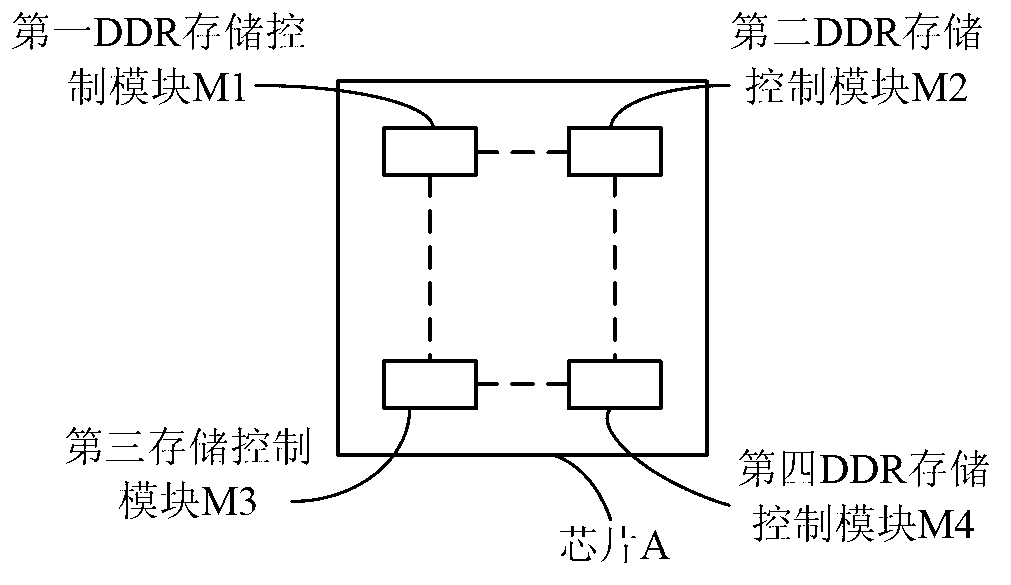
[0031] figure 1 It schematically shows the arrangement of the DDR storage control module on the DDR signal wiring package substrate according to the first embodiment of the present invention.

[0032] Such as figure 1 As shown, the DDR signal wiring packaging substrate according to the first embodiment of the present invention includes: a plurality of DDR storage control modules placed symmetrically on chip A of the DDR signal wiring packaging substrate. In this embodiment, the multiple DDR storage control modules include a first DDR storage control module M1, a second DDR storage control module M2, a third DDR storage control module M3, and a fourth DDR storage control module M4, wherein the first DDR storage The control module M1 , the second DDR storage control module M2 , the third DDR storage control module M3 and the fourth DDR storage control module M4 are located at the four corners of a square, thus forming a perfect symmetrical arrangement.

[0033] figure 2 It s...

no. 2 example

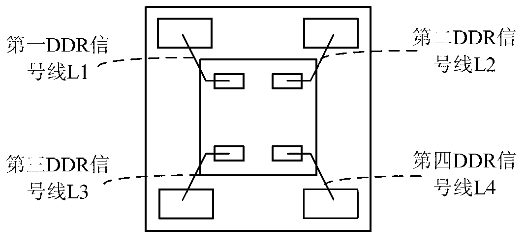
[0042] Figure 4 The layout of the DDR signal layer of the DDR signal wiring package substrate according to the second embodiment of the present invention is schematically shown.

[0043] Such as Figure 4 As shown, the DDR signal wiring package substrate according to the second embodiment of the present invention includes: a sequentially stacked ground plane layer 1, a first dielectric layer 2, a DDR signal layer 3, a second dielectric layer 4, and a DDR interface power plane layer 5 . Wherein, the DDR interface power plane layer 5 and the ground plane layer 1 are selected as the reference plane layer of the DDR signal at the same time.

[0044] On the DDR signal wiring package substrate according to the second embodiment of the present invention, a stacked structure such as the DDR interface power plane layer / DDR high-speed signal / ground plane layer is adopted, and the DDR interface power plane layer and the ground plane layer are selected as the DDR The reference plane l...

no. 3 example

[0047] Figure 5 A DDR signal wiring package substrate according to a third embodiment of the present invention is schematically shown.

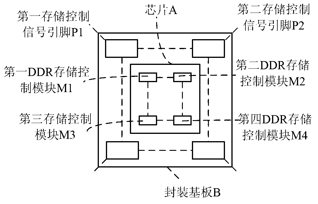
[0048] The DDR signal wiring package substrate according to the third embodiment of the present invention further includes: a plurality of DDRs formed by correspondingly connecting one of the plurality of DDR storage control modules to one of the plurality of storage control signal pins. Signal vias.

[0049] The DDR signal wiring package substrate according to the third embodiment of the present invention further includes: a plurality of ground holes arranged symmetrically with reference to the positions of the plurality of DDR signal via holes.

[0050] More specifically, in this embodiment, the first DDR signal via hole W1, the second DDR signal via hole W2, the third DDR signal via hole W3 and the fourth DDR signal via hole W4 are formed; correspondingly refer to the first The positions of the DDR signal via hole W1, the second DDR sig...


PUM


Abstract

The invention provides a double data rate (DDR) signal wiring encapsulation substrate and a DDR signal wiring encapsulation method. A plurality of DDR storage control modules are symmetrically arranged on a chip. A plurality of storage control signal pins corresponding to the DDR storage control module are symmetrically arranged in the area outside the chip. A plurality of DDR signal wires which are symmetrically distributed are used for respectively and correspondently joining one of the DDR storage control modules to one of the storage control signal pins. The DDR signal wiring encapsulation substrate comprises a ground plane layer, a first medium layer, a DDR signal layer, a second medium layer and a DDR interface power supply plane layer; and the DDR interface power supply plane layer and the ground plane layer are simultaneously selected as a reference plane layer of a DDR signal. The DDR storage control modules are respectively and correspondently connected to the storage control signal pins through a plurality of DDR signal holes which are symmetrically distributed. A plurality of ground holes are correspondently and symmetrically distributed referring to the positions of the DDR signal holes.

Description

technical field [0001] The invention relates to semiconductor packaging technology, more specifically, the invention relates to a DDR signal wiring packaging substrate and a DDR signal wiring packaging method. Background technique [0002] Almost every electronic device, from smartphones to servers, uses some form of RAM (Random Access Memory) storage. Due to the relatively low cost per bit of SDRAM (Synchronous Dynamic Random Access Memory), it provides a good combination of speed and storage. Therefore, SDRAM remains the mainstream memory technology for most computers and computer-based products. [0003] DDR (Double Data Rate) is a double data rate SDRAM memory, which has become the choice of memory technology today. DDR technology continues to evolve, increasing speed and capacity while reducing cost, power, and the physical size of storage devices. [0004] DDR is also called DDR SDRAM (Double Rate Synchronous Dynamic Random Access Memory), which is simply called DDR...

Claims


Application Information

Patent Timeline
Patent Type & Authority Applications(China)
IPC IPC(8): H01L23/498H01L23/12H01L21/58H01L21/60
CPCH01L2924/3011H01L2224/49171H01L2924/30107H01L2924/00
Inventor 胡晋丁亚军金利峰李川王玲秋王彦辉
Owner JIANGNAN INST OF COMPUTING TECH
Why Eureka
Try Eureka