
Storage element and storage device

A storage element and storage layer technology, applied in the field of storage devices and storage elements, can solve the problems of energy consumption reduction, capacity increase, etc., to reduce energy consumption, reduce reverse current, suppress thermal stability and reverse current changes Effect

Active Publication Date: 2012-11-28
SONY CORP
View PDF9 Cites 5 Cited by
  • Summary
  • Abstract
  • Description
  • Claims
  • Application Information

AI Technical Summary

Problems solved by technology

Due to its high-speed operation and high reliability, MRAM is expected to be extended to code storage and working memory in the future; however, in practice, there are still problems such as reduction in power consumption and increase in capacity to be overcome
The above-mentioned problem is inherent in the recording principle of MRAM, that is, it is caused by the method of magnetization reversal by the current magnetic field generated by wiring

Method used


Image

  • Storage element and storage device
  • Storage element and storage device
  • Storage element and storage device

Examples


Embodiment Construction

[0034] Hereinafter, embodiments of the present invention will be described in the following order.

[0035]

[0036]

[0037]

[0038]

[0039]

[0040]

[0041]

[0042] First, the structure of the storage device according to the embodiment will be described.

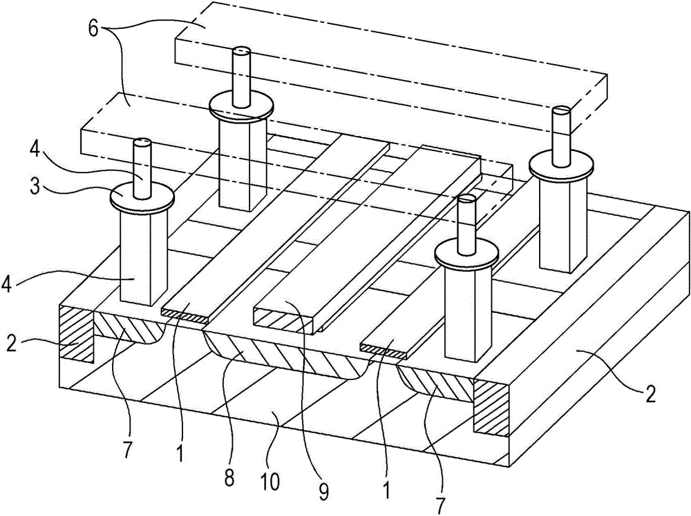
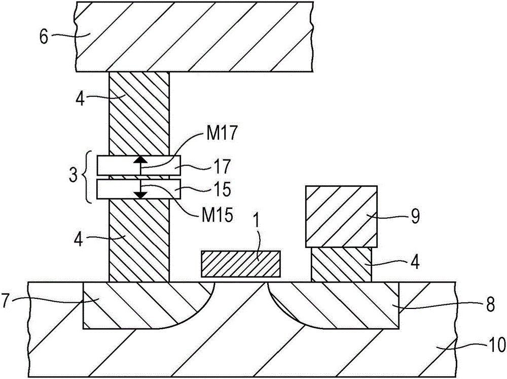
[0043] exist figure 1 and 2 A schematic diagram of a storage device according to an embodiment is shown in . figure 1 for the perspective view, figure 2 is a cross-sectional view.

[0044] Such as figure 1 As shown, in the storage device according to the embodiment, the storage element 3 of the ST-MRAM capable of retaining information by the magnetization state is arranged at the intersection of two types of address lines (such as word lines and bit lines) that perpendicularly intersect point nearby.

[0045]That is, a drain region 8, a source region 7, and a gate electrode 1 forming a selection transistor for selecting each memory device are formed in a region isolated by an element isolation laye...


PUM

PropertyMeasurementUnit
thicknessaaaaaaaaaa
diameteraaaaaaaaaa
diameteraaaaaaaaaa

Abstract

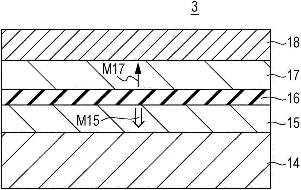
A storage element includes: a storage layer which retains information by a magnetization state of a magnetic substance; a magnetization pinned layer having magnetization which is used as the basis of the information stored in the storage layer; and an interlayer of a non-magnetic substance provided between the storage layer and the magnetization pinned layer. The storage element is configured to store information by reversing magnetization of the storage layer using spin torque magnetization reversal generated by a current passing in a laminate direction of a layer structure including the storage layer, the interlayer, and the magnetization pinned layer, and when the saturation magnetization of the storage layer and the thickness thereof are represented by Ms (emu / cc) and t (nm), respectively, (1489 / Ms)-0.593<t<(6820 / Ms)-1.55 holds.

Description

technical field [0001] The present invention relates to a memory element that has a plurality of magnetic layers and performs recording using spin torque magnetization reversal, and a memory device using the same. Background technique [0002] Accompanying the significant development of various information devices including such as mobile terminals, large-capacity servers, etc., the elements (such as memory and logic circuits) forming these devices are also required to improve performance, such as an increase in the degree of integration, an increase in operating speed, and reduction in power consumption. reduce. In particular, the advancement of nonvolatile semiconductor memory has been prominent, and there is an increasing demand for flash memory serving as large-capacity file storage instead of hard disk drives. [0003] In addition, considering the expansion of code storage and work memory, in order to replace the NOR flash memory, DRAM, etc. that are commonly used toda...

Claims


Application Information

Patent Timeline
Patent Type & Authority Applications(China)
IPC IPC(8): H01L43/08G11C11/16H01F10/32B82Y25/00
CPCH01L43/08H01F10/3286G11C11/16H01L27/228H01F10/329G11C11/161H10B61/22H10N50/10H10B61/00H10N50/01
Inventor 肥后丰细见政功大森广之别所和宏浅山徹哉山根一阳内田裕行
Owner SONY CORP
Learn More