Low-power-consumption time delay integral type CMOS (Complementary Metal-Oxide-Semiconductor Transistor) image sensor

A technology of time-delay integration and image sensor, which is applied in the field of reducing the power consumption of time-delay integration (TDI) type CMOS image sensor and low power consumption time-delay integration type CMOS image sensor, which can solve the power consumption of analog-to-digital conversion circuit advanced questions

Inactive Publication Date: 2012-11-28
TIANJIN UNIV
View PDF3 Cites 30 Cited by
  • Summary
  • Abstract
  • Description
  • Claims
  • Application Information

AI Technical Summary

Problems solved by technology

[0010] For the digital domain accumulation mode, the accumulation process is realized by digital circuits, and the accumulation process will not cause a lot of power consumption, but the digital domain accumulation needs to convert the CDS signal into a digital signal first. If this process is limited to a very short time completed, the power consumption of the corresponding analog-to-digital conversion circuit is also very high, and usually the power consumption of the analog-to-digital conversion circuit also occupies a large part of the power consumption of the entire digital domain TDI-CMOS image sensor

Method used


Image

  • Low-power-consumption time delay integral type CMOS (Complementary Metal-Oxide-Semiconductor Transistor) image sensor
  • Low-power-consumption time delay integral type CMOS (Complementary Metal-Oxide-Semiconductor Transistor) image sensor
  • Low-power-consumption time delay integral type CMOS (Complementary Metal-Oxide-Semiconductor Transistor) image sensor

Examples


Embodiment Construction

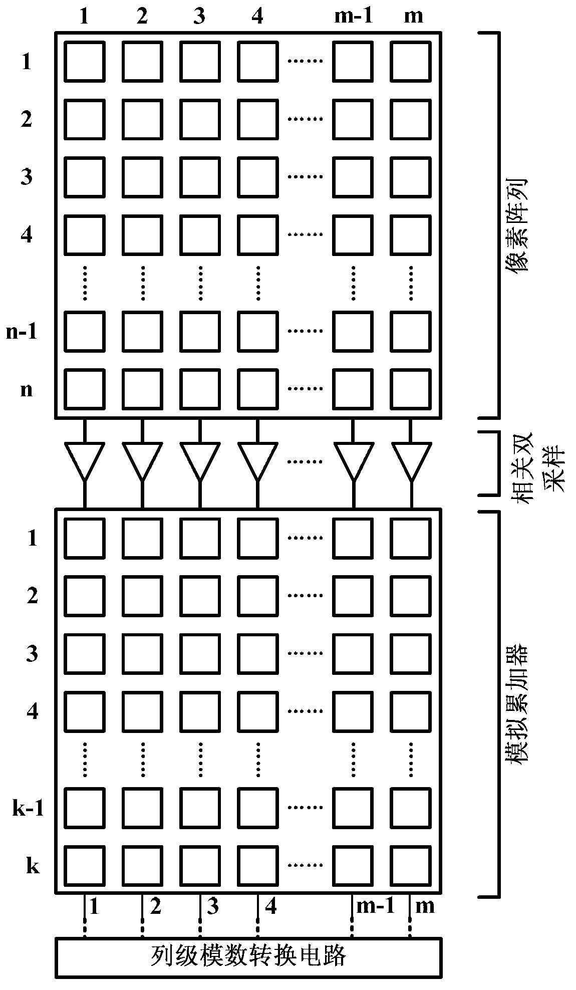
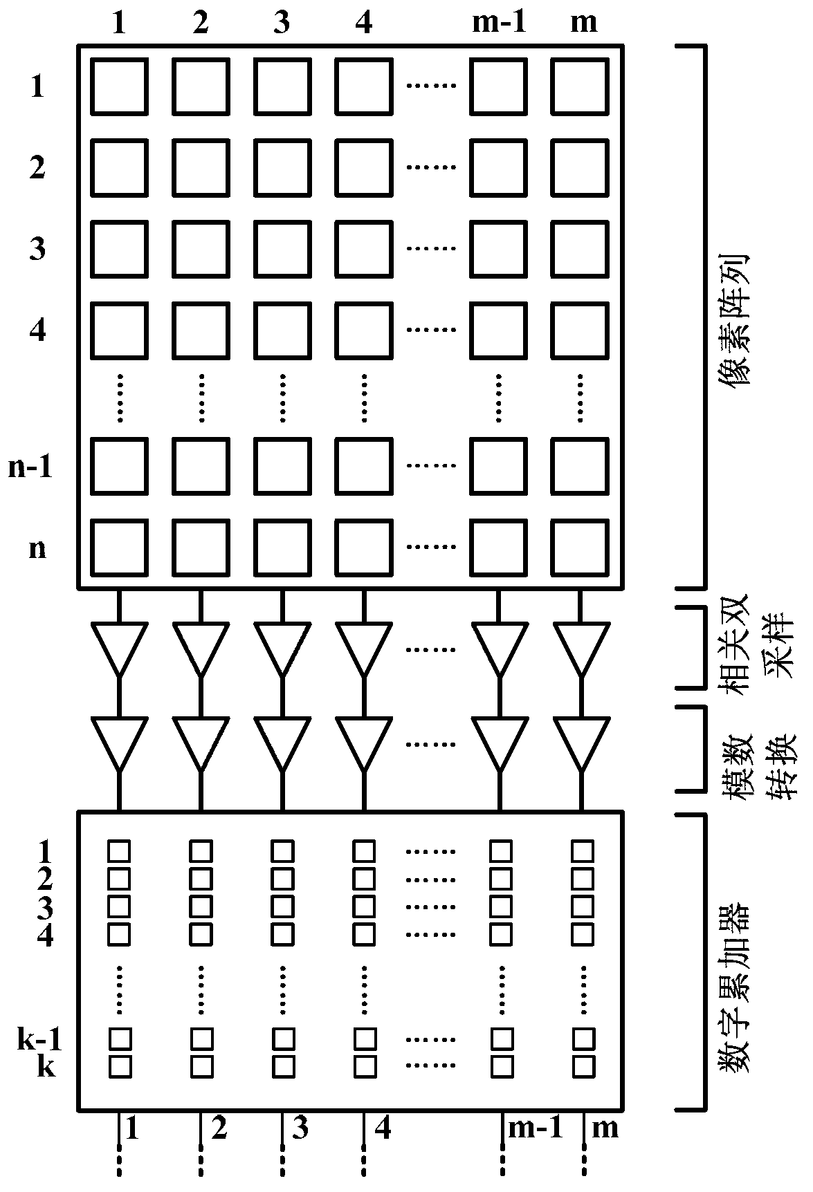
[0030] The present invention proposes an accumulation mode in which the internal charge domain accumulation of the pixel is combined with the external accumulation of the pixel. By reducing the number of external accumulations of the pixel array, the establishment time of the operational amplifier in the external analog domain accumulation mode can be extended, or the external digital domain accumulation can be prolonged. The purpose of the analog-to-digital conversion time in the mode, thereby greatly reducing the power consumption of the entire TDI-CMOS image sensor.

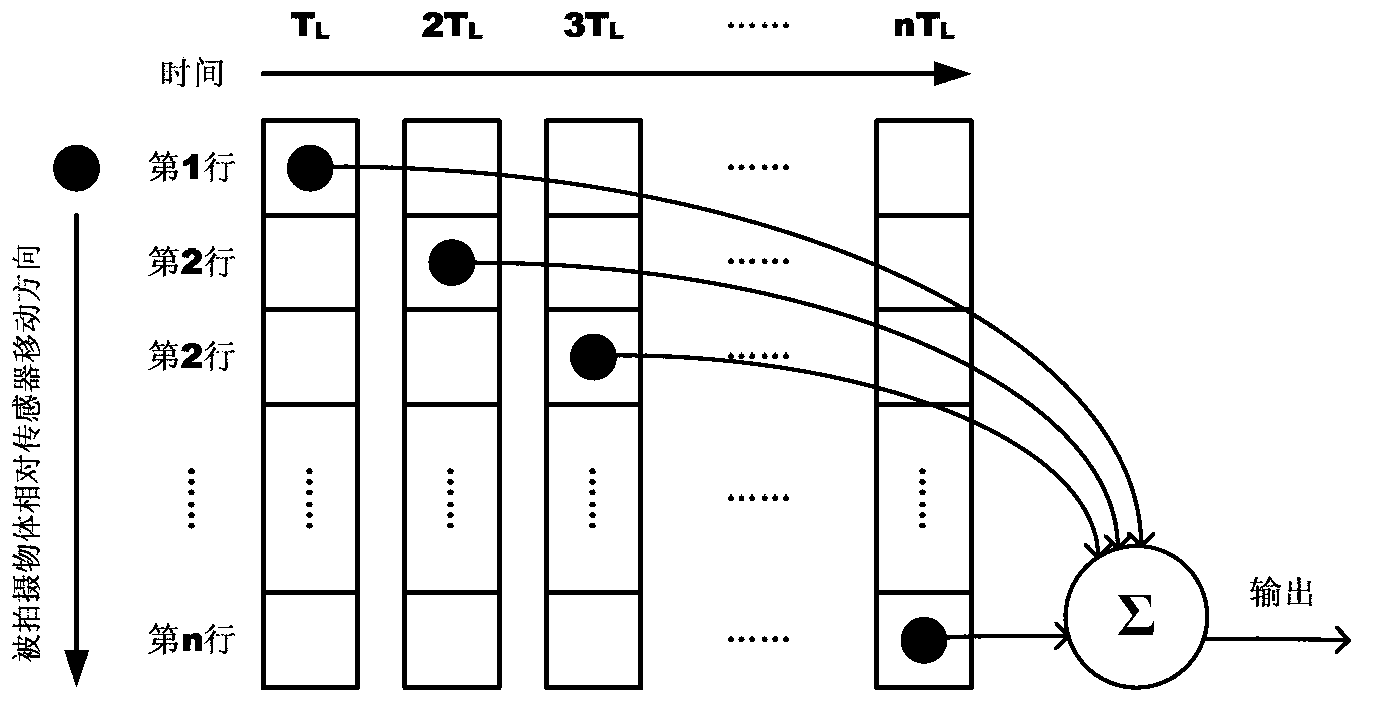
[0031] TDI-type CMOS image sensors mostly adopt a drum-type exposure method, that is, the signals of each row of the pixel array are read out sequentially. For a pixel array with N rows of pixels, during the movement of the sensor relative to the object to be photographed, the object image of the object is sequentially projected into the pixels in the 1st, 2nd, 3rd...N-1, Nth rows. The optional readout sequenc...


PUM


Abstract

The invention relates to a method for reducing power consumption of an image sensor. In order to achieve the aim of greatly reducing the power consumption of a whole TDI-CMOS (Transport Driver Interface-Complementary Metal-Oxide-Semiconductor Transistor) image sensor, the technical scheme disclosed by the invention is as follows: the invention provides a low-power-consumption time delay integral type CMOS image sensor; a pixel array adopts a manner of drum-type exposure and under-sampling; adjacent two rows of each array of the pixel array form one group and each group is provided with a storage node; a first row of pixels of the pixel array collect photoelectric charges generated by object F exposure and transfer the photoelectric charges to the storage node; and then a second row of the pixels collect the photoelectric charges generated by the object F exposure and charges corresponding to an object F in the storage node, and transfer the charges to a charge-voltage conversion node, so that one time of charge accumulation is finished and a voltage signal for subsequent circuit processing can be generated at the same time; and a third row of the pixels, a fourth row of the pixels and subsequent each row of the pixels are subjected to the steps. The method disclosed by the invention is mainly used for designing and manufacturing the image sensor.

Description

technical field [0001] The present invention relates to a method for reducing the power consumption of a complementary metal oxide semiconductor (CMOS) image sensor, in particular to a method for reducing the power consumption of a time-delay integration (TDI) type CMOS image sensor, specifically, a low-power time delay Integrating CMOS image sensor. Background technique [0002] The image sensor can convert the optical signal obtained by the lens into an electrical signal that is easy to store, transmit and process. Image sensors can be divided into area array type and line array type according to the working method. The working principle of the area array image sensor is to shoot an object with a pixel array arranged in a two-dimensional array to obtain two-dimensional image information, while the working principle of the line array image sensor is to use a pixel array arranged in a one-dimensional line array Two-dimensional image information is obtained by scanning and ...

Claims


Application Information

Patent Timeline
Patent Type & Authority Applications(China)
IPC IPC(8): H04N5/374H04N5/3745H04N5/378H04N5/351
Inventor 姚素英徐超高静徐江涛史再峰
Owner TIANJIN UNIV
Why Eureka
Try Eureka