
Forming method for variable resistance non-volatile memory element and variable resistance non-volatile memory device

A non-volatile storage and resistance change technology, which is applied to the shaping of resistance change type non-volatile memory elements and the fields of resistance change type non-volatile memory devices, can solve the problem of increasing the shaping voltage of resistance change elements and shaping the voltage. deviations, etc.

Active Publication Date: 2012-11-28
PANASONIC SEMICON SOLUTIONS CO LTD
View PDF6 Cites 7 Cited by
  • Summary
  • Abstract
  • Description
  • Claims
  • Application Information

AI Technical Summary

Problems solved by technology

[0039] However, in the above-mentioned conventional variable resistance semiconductor memory device, there is a technical problem in that the shaping voltage varies for each variable resistance element constituting the memory cell array, or that in order to transition to the state where the resistance change starts, the Initially, the shaping voltage applied to the variable resistance element increases

Method used


Image

  • Forming method for variable resistance non-volatile memory element and variable resistance non-volatile memory device
  • Forming method for variable resistance non-volatile memory element and variable resistance non-volatile memory device
  • Forming method for variable resistance non-volatile memory element and variable resistance non-volatile memory device

Examples


Embodiment Construction

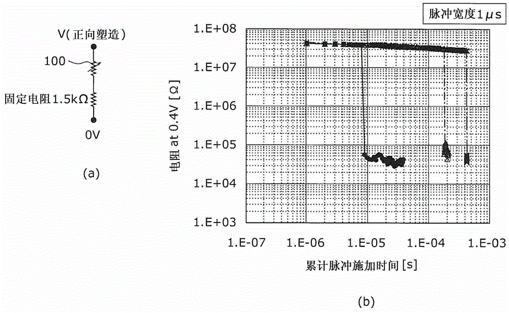
[0117] First, for Figure 29 The shown 1T1R type memory cell composed of a variable resistance element shows molding characteristics for the case where Pt (platinum) is used in the upper electrode 100c and the case where Ir (iridium) is used for the upper electrode 100c, And explain its technical problems, wherein the variable resistance element is composed of the first transition metal oxide layer 100b-1 (here, TaO x , 0y , x<y) to form.

[0118] Here, in the sample used in the experiment, the area of ​​the variable resistance layer 100b is 0.25 μm 2 (=0.5μm×0.5μm), having a first transition metal oxide layer 100b-1 (here, TaO x : X=1.54, film thickness: 44.5nm), and the second transition metal oxide layer 100b-2 (here, TaO y : y=2.47, film thickness: 5.5 nm). The NMOS transistor serving as a switching element has a gate width W: 0.44 μm, a gate length L: 0.18 μm, and a gate insulating film thickness Tox: 3.5 nm.

[0119] The second transition metal oxide layer 100b-2 (h...


PUM


Abstract

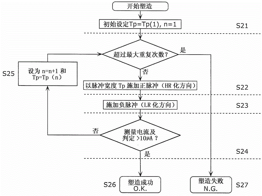
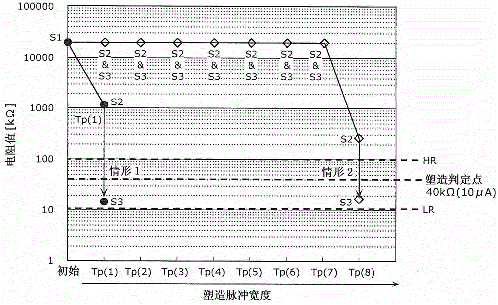
Disclosed is a forming method for a variable resistance non-volatile memory element which provides lower forming voltage than conventional methods and whereby variation in forming voltage between individual variable resistance elements can be avoided. The forming method initializes a variable resistance element (100) and includes a step (S24) that determines whether or not a 1T1R memory cell current is larger than a reference current; a step (22) that, when the current is determined to be larger (i.e., "No" in S24), applies a positive voltage pulse for forming whereby the pulse width (Tp (n)) is stepped up; and a step (S23) that applies a negative voltage pulse with a pulse width (Tn) at or below the pulse width Tp (n). The step S24 and the voltage application steps S22 and S23 are repeated until the forming has been completed.

Description

technical field [0001] The present invention relates to a molding (initialization) method for stably performing resistance change in a variable resistance nonvolatile memory element, and a variable resistance nonvolatile memory device having such a function, wherein the variable resistance nonvolatile memory element The volatile memory element reversibly changes its resistance value based on an electrical signal. Background technique [0002] In recent years, variable resistance nonvolatile memory devices (hereinafter also simply referred to as "Non-volatile memory device") research and development. The variable resistance element refers to an element that has a property of reversibly changing a resistance value according to an electric signal, and can store data corresponding to the resistance value in a non-volatile manner. [0003] As a nonvolatile memory device using a variable resistance element, it is generally known that a MOS transistor and a variable resistance el...

Claims


Application Information

Patent Timeline
Patent Type & Authority Applications(China)
IPC IPC(8): G11C13/00H01L27/10H01L45/00H01L49/00
CPCG11C2213/32H01L45/146G11C2013/0083G11C13/0007H01L45/1233G11C2213/79H01L27/101G11C13/0069H01L27/2436H01L45/08H01L45/16G11C2013/0073H10B63/30H10N70/24H10N70/011H10N70/826H10N70/8833
Inventor 河合贤岛川一彦片山幸治
Owner PANASONIC SEMICON SOLUTIONS CO LTD
Learn More