Supercharge Your Innovation With Domain-Expert AI Agents!

Semiconductor device

A semiconductor and conductive technology, which is applied in the direction of semiconductor devices, semiconductor/solid-state device manufacturing, transistors, etc., can solve the problem of on-state voltage reduction, achieve the effect of reducing reverse recovery current and preventing component damage

Inactive Publication Date: 2012-11-28
TOYOTA JIDOSHA KK
View PDF4 Cites 12 Cited by
  • Summary
  • Abstract
  • Description
  • Claims
  • Application Information

AI Technical Summary

Problems solved by technology

As a result, the on-state voltage during IGBT operation decreases

Method used


Image

  • Semiconductor device
  • Semiconductor device
  • Semiconductor device

Examples


Embodiment 1

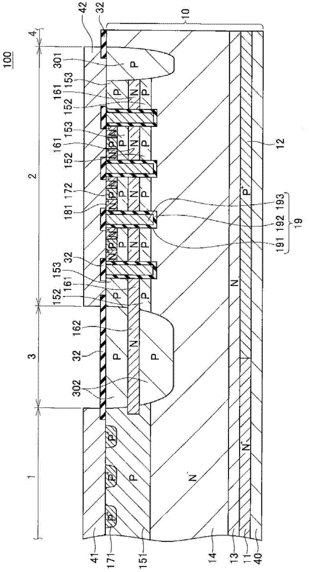
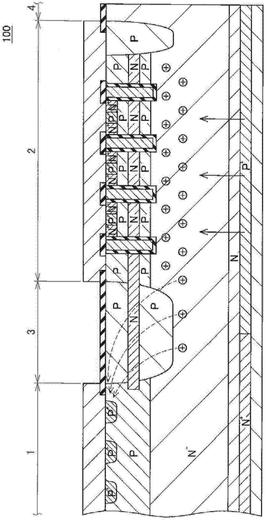
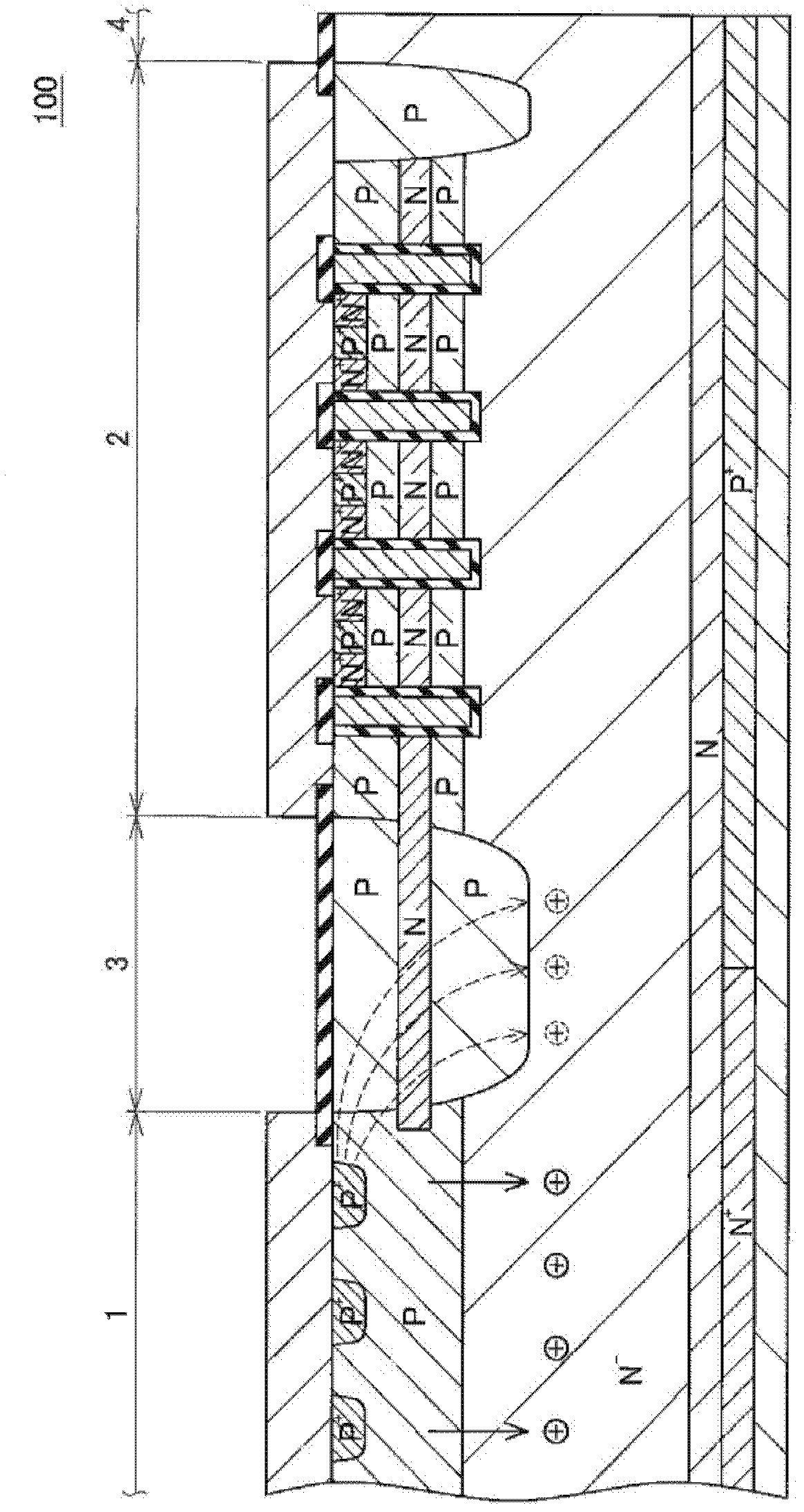
[0019] Hereinafter, Embodiment 1 of the present invention will be described with reference to the drawings. In this embodiment, a case where the first conductivity type is set as P type and the second conductivity type is set as N type will be described as an example. figure 1 is a cross-sectional view of the semiconductor device 100 according to this embodiment. figure 2 for, modeled figure 1 A diagram of the state of the semiconductor device 100 when the IGBT is operating as shown in image 3 for, modeled figure 1 A diagram showing the state of the semiconductor device 100 when the diode is operating. exist figure 2 , image 3 in, right in figure 1 The symbols of the respective structures of the semiconductor device 100 shown in . exist figure 2 , image 3 In , a plus sign surrounded by a circle indicates a hole.

[0020] The semiconductor device 100 has a semiconductor substrate 10 , a back electrode 40 , a diode front surface electrode 41 , and an IGBT front s...


PUM


Abstract

Disclosed is a semiconductor device comprising an IGBT element region, a diode element region, and a boundary region provided between the IGBT element region and the diode element region, the IGBT element region, the diode element region and the boundary region being provided within an identical semiconductor substrate. A second conductivity type carrier accumulation region is provided within a first conductivity type first body region in the IGBT element region. In the boundary region, a second conductivity type third diffusion region is provided within the first conductivity type second diffusion region so as to extend by such a length that the second conductivity type third diffusion region comes into contact with the carrier accumulation region. The above constitution can suppress the movement of carriers through the boundary region into the diode element region during the actuation of IGBT to reduce an on-voltage. Further, in diode reverse recovery, the accumulation of carriers in a drift region in the boundary region can be suppressed to reduce a reverse recovery current.

Description

technical field [0001] The present invention relates to a semiconductor device in which an insulated gate bipolar transistor (IGBT) element region and a diode element region are formed on the same semiconductor substrate. Background technique [0002] Patent Document 1 discloses a semiconductor device in which an IGBT element region and a diode element region for reflow are formed on the same semiconductor substrate. On the semiconductor substrate, the back side, N - layer, N layer, P layer. N is provided on a part of the surface of the P layer + layer. Provided with the P layer and the N layer from the surface side of the semiconductor substrate to reach the N layer. - layers of trench gates. trench gate with N + The layers are connected. As the back layer, while formed with P + Layer or N + layer. The backside layer becomes P + The area of ​​the layer is the IGBT element area, while the back layer becomes the N + The area of ​​the layer is the diode element are...

Claims


Application Information

Patent Timeline
Patent Type & Authority Applications(China)
IPC IPC(8): H01L21/76H01L21/8234H01L27/04H01L27/06H01L27/088H01L29/739H01L29/78
CPCH01L29/8611H01L27/0664H01L29/7397H01L29/0834H01L29/1095H01L27/088H01L29/739
Inventor 添野明高
Owner TOYOTA JIDOSHA KK
Features
  • R&D
  • Intellectual Property
  • Life Sciences
  • Materials
  • Tech Scout
  • Unparalleled Data Quality
  • Higher Quality Content
  • 60% Fewer Hallucinations
Learn More