Thin-film process system with wafer storage groove and wafer accessing method thereof

A thin-film process and process technology, which is applied in the manufacture of conveyor objects, electrical components, semiconductor/solid-state devices, etc., can solve the problems of mutual pollution between chips and long waiting time, etc., to reduce waiting time and improve product performance and quality , the effect of avoiding potential risks

Active Publication Date: 2015-02-11
SHANGHAI HUALI MICROELECTRONICS CORP
View PDF4 Cites 0 Cited by
  • Summary
  • Abstract
  • Description
  • Claims
  • Application Information

AI Technical Summary

Problems solved by technology

[0008] The present invention aims at the fact that in the prior art, the wafer in the traditional thin film process system waits too long in the wafer box under the atmospheric atmosphere, so it is easy to combine with water vapor in the air and adsorb some highly active substances. Or the volatilization of the residual chemical reagents of the wafer itself after the thin film process causes defects such as mutual contamination between the wafers, and a thin film process system with a storage slot is provided

Method used


Image

  • Thin-film process system with wafer storage groove and wafer accessing method thereof
  • Thin-film process system with wafer storage groove and wafer accessing method thereof
  • Thin-film process system with wafer storage groove and wafer accessing method thereof

Examples


Embodiment Construction

[0031] In order to illustrate the technical content, structural features, achieved goals and effects of the present invention in detail, the following will be described in detail in conjunction with the embodiments and accompanying drawings.

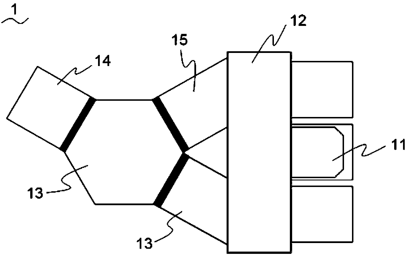
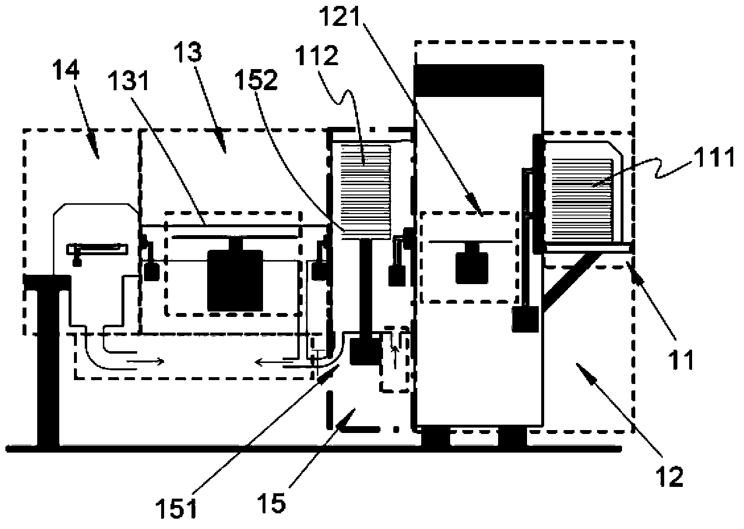
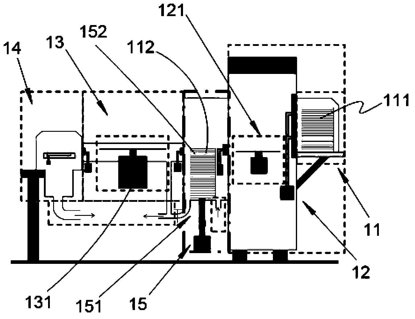
[0032] see figure 1 , figure 2 , image 3 , figure 1 Shown is a top view structure schematic diagram of the thin film processing system with a storage slot of the present invention. figure 2 Shown is a side view structure diagram of the thin film process system with a storage slot in the present invention with the storage slot located at the upper end. image 3 Shown is a side view structure schematic diagram of the thin film process system with a storage slot in the present invention, where the storage slot is located at the lower end. The thin film process system 1 with the storage tank includes a wafer storage unit 11, a wafer transfer chamber 12, a vacuum feeding chamber 13, and a process chamber 14 connected sequentially in ...


PUM


Abstract

The invention relates to a thin-film process system with a wafer storage groove. The system comprises a wafer storage unit, a wafer transfer cavity, a vacuum wafer conveying cavity, a process cavity and a vacuum wafer storage cavity arranged between the wafer conveying cavity and the vacuum conveying cavity connected in sequence successively. The vacuum wafer storage cavity further comprises a pumping unit communicated with the vacuum wafer storage cavity. The pumping unit is used to provide a vacuum atmosphere or an air atmosphere for the vacuum wafer storage cavity. The wafer storage groove is moveably arranged in the vacuum wafer storage cavity. According to the thin-film process system with the wafer storage groove provided by the invention, the vacuum wafer storage cavity with the moveably arranged wafer storage groove is additionally arranged so that not only the waiting time of risk of processed wafers is effectively reduced, but also mutual influence between wafers after thin-film process and wafers to be processed is avoided, and potential risks are avoided and the performance and quality of products are improved.

Description

technical field [0001] The invention relates to the technical field of semiconductor devices, in particular to a thin film process system with a chip storage slot and a chip access method thereof. Background technique [0002] With the development of semiconductor device technology and proportional size reduction, the complexity of the process flow and production difficulty are constantly increasing, and the requirements for the production environment are also getting higher and higher. The production environment includes two aspects: first, the clean room environment for semiconductor device production; second, the local environment inside the semiconductor device production equipment. The pros and cons of the above two aspects of the environment directly affect the performance and quality of semiconductor products. [0003] see Figure 5 , Figure 5 Shown is a schematic top view of the dry etching equipment of the thin film process system in the prior art. The working me...

Claims


Application Information

Patent Timeline
Patent Type & Authority Patents(China)
IPC IPC(8): H01L21/67H01L21/677H01L21/02
Inventor 黄海
Owner SHANGHAI HUALI MICROELECTRONICS CORP
Why Eureka
Try Eureka