Display device, and method for producing array substrate for display device

A technology of a display device and a manufacturing method, applied in the directions of identification devices, optics, instruments, etc.

Inactive Publication Date: 2012-12-12
SHARP KK
View PDF6 Cites 10 Cited by
  • Summary
  • Abstract
  • Description
  • Claims
  • Application Information

AI Technical Summary

Problems solved by technology

However, in the current manufacturing process of thin-film transistor substrates (TFT substrates) for large-scale LCD TVs, at least four to five photolithography processes and two CVD (Chemical Vapor Deposition: Chemical Vapor Deposition) processes are required for film formation.
These treatments become the substantial boundaries of process-saving

Method used


Image

  • Display device, and method for producing array substrate for display device
  • Display device, and method for producing array substrate for display device
  • Display device, and method for producing array substrate for display device

Examples


Embodiment Construction

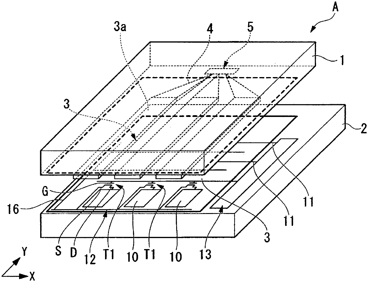
[0225] Below, while referring to the attached Figure 1 One embodiment of the display device of the present invention will be described.

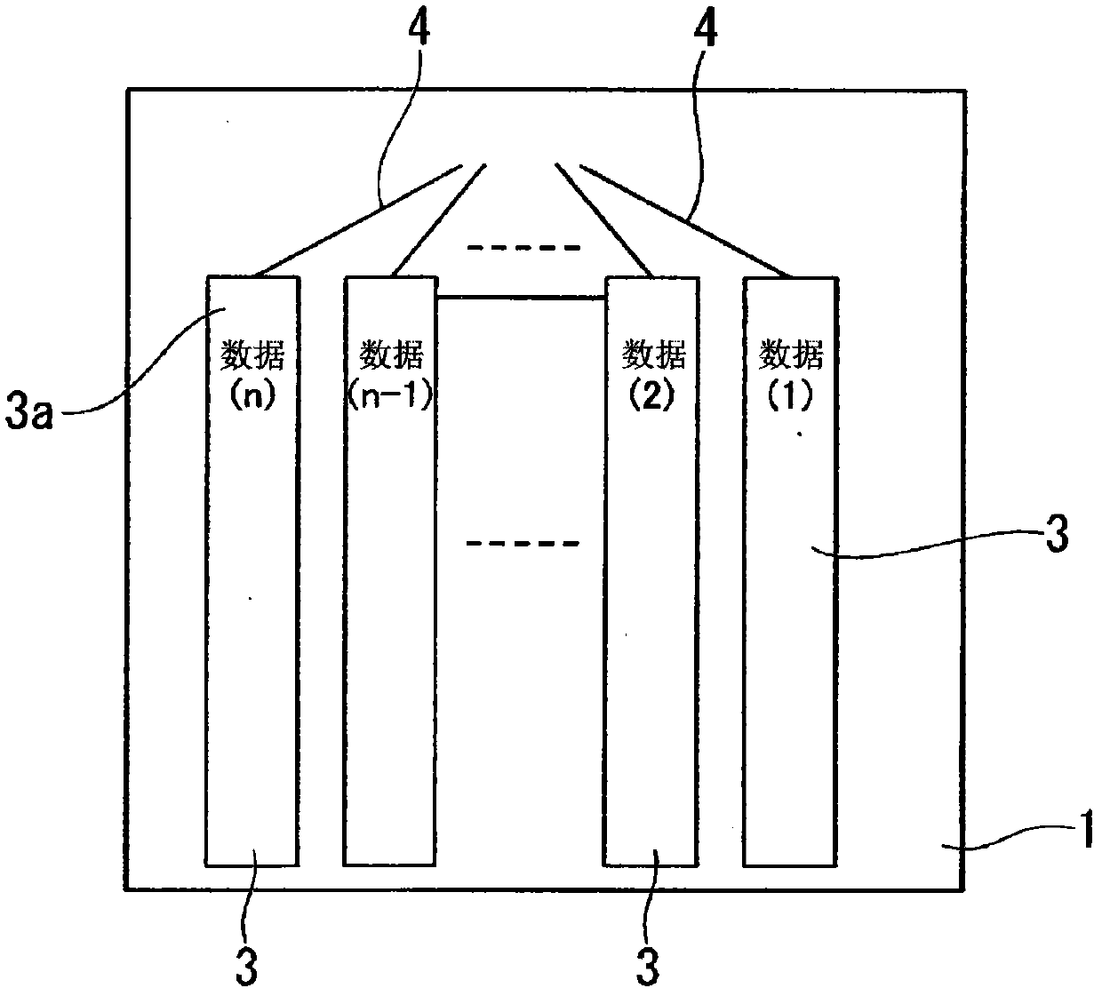
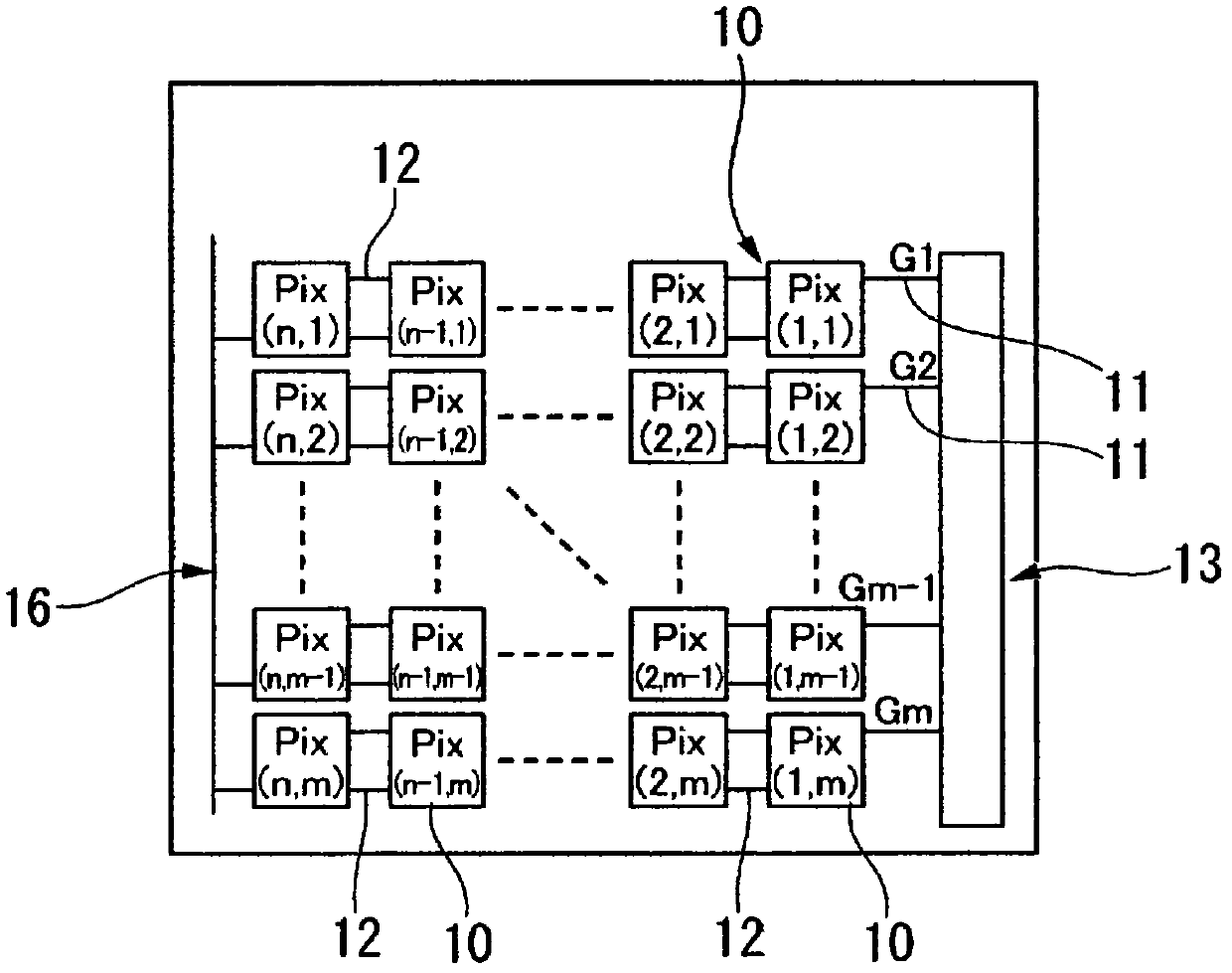
[0226] The display device of the present embodiment is applied to a relative data supply type display device in which a display medium layer such as a liquid crystal layer is sandwiched between a pair of substrates. figure 1 It is a figure which shows the outline|summary of both board|substrates and the wiring formed on both board|substrates in the state which made both board|substrates face each other. figure 2 It is a diagram showing the wiring of the opposite substrate. image 3 It is a diagram showing the wiring of the element-side substrate. Figure 4 It is a diagram showing a wiring structure around a pixel electrode. Figure 5 It is a schematic diagram showing an overall circuit of a display device in which both substrates are combined. Figure 6A and Figure 6B It is a configuration diagram showing an example of a thin film t...


PUM

PropertyMeasurementUnit
thicknessaaaaaaaaaa

Abstract

Disclosed is a display device provided with: a plurality of stripe-shaped data electrodes (3) which are formed on a first substrate (1) and which extend in the vertical direction; a plurality of scanning lines (11) and a plurality of reference signal lines (12) which are formed on the second substrate (2) and which extend in the horizontal direction; a plurality of pixel electrodes (10) which are formed on the second substrate (2) and which are arranged in the form of a matrix; a plurality of switching elements (T1) which are formed on the second substrate (2), turns on or off by means of the plurality of scanning lines (11), and is disposed between the plurality of reference signal lines (12) and the plurality of pixel electrodes (10); and an oxide semiconductor layer (22) which is disposed between a source electrode (21) and a drain electrode (20). The oxide semiconductor layer (22) is formed with the switching elements (T1) with an insulating layer (23) therebetween in the vicinity of a gate electrode (11a), and is provided with the pixel electrodes (10) which are connected to the source electrode (21) or the drain electrode (20). The source electrode (21) or the drain electrode (20) that is connected to the pixel electrode (10) is formed from the same material as the pixel electrode (10). The source electrode (21) and the drain electrode (20) are formed from a film which was formed at the same time.

Description

technical field [0001] The present invention relates to a display device using an oxide semiconductor as a switching element and a method for manufacturing an array substrate for the display device. [0002] This application claims priority based on Japanese Patent Application No. 2010-072382 for which it applied in Japan on March 26, 2010, and uses the content here. Background technique [0003] In order to reduce the cost of a large LCD TV equipped with an active-matrix-driven LCD panel, process-saving is effective. However, in the current manufacturing process of thin-film transistor substrates (TFT substrates) for large-scale LCD TVs, at least four to five photolithography processes and two CVD (Chemical Vapor Deposition: Chemical Vapor Deposition) processes are required for film formation. These treatments become substantial boundaries of process-saving. [0004] A thin film transistor provided on a TFT substrate requires at least three types of electrodes (source ele...

Claims


Application Information

Patent Timeline
Patent Type & Authority Applications(China)
IPC IPC(8): G09F9/30G02F1/1368H01L21/28H01L29/417H01L29/786
CPCH01L27/1214H01L27/1288G02F1/136286H01L27/1225H01L29/41733G02F1/1368H01L27/124
Inventor 镰田豪青森繁井出哲也大桥诚二胜田升平
Owner SHARP KK
Why Eureka
Try Eureka