A manufacturing process of copper interconnection wire

A manufacturing process and interconnection technology, which is applied in semiconductor/solid-state device manufacturing, electrical components, circuits, etc., to achieve the effect of increasing productivity, reducing etching steps, and reducing manufacturing costs

Active Publication Date: 2015-08-19
SHANGHAI HUALI MICROELECTRONICS CORP
View PDF2 Cites 0 Cited by
  • Summary
  • Abstract
  • Description
  • Claims
  • Application Information

AI Technical Summary

Problems solved by technology

Since the double patterning technology requires two photolithography and etching, its cost is much higher than the traditional single exposure forming technology

Method used


Image

  • A manufacturing process of copper interconnection wire
  • A manufacturing process of copper interconnection wire
  • A manufacturing process of copper interconnection wire

Examples


Embodiment Construction

[0030] The specific embodiment of the present invention will be further described below in conjunction with accompanying drawing:

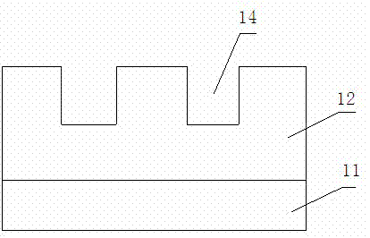
[0031] Figures 3a-3i It is a schematic structural flow diagram of a manufacturing process of a copper interconnection wire of the present invention;

[0032] Such as Figures 3a-3i As shown, a manufacturing process of a copper interconnection in the present invention, first, deposit a low dielectric constant dielectric layer 32 on the upper surface of a silicon substrate 31, and coat the first photoresist 33 that can form a hard mask to cover the dielectric layer 32, after exposure and development, the excess photoresist is removed to form a first hard mask photoresist 331 with a metal groove structure 34; wherein, the material of the first photoresist 33 contains silane groups, silane oxides Base or clathrate siloxane, etc.

[0033] Secondly, in the same developing station, coating liquid silylation material 35 such as hexamethyldisilazane, t...


PUM


Abstract

The invention relates to the manufacturing field of semiconductors, in particular to a manufacturing process for a copper interconnection line. According to the manufacturing process for the copper interconnection line disclosed by the invention, silanization materials are adopted in a trench-preference copper interconnection process to form an isolating film between two layers of photoresists in a dual-exposure technology, and through holes and metal trench structures in the photoresists are transferred to dielectric layers in sequence, so that the existing process, in which the etching of the metal trench and the etching of the through hole are carried out in two independent steps, can be replaced, the etching steps in dual-Damascus metal interconnection line process are effectively reduced, the production capacity is increased and the manufacturing cost is reduced.

Description

technical field [0001] The invention relates to the field of semiconductor manufacturing, in particular to a manufacturing process of copper interconnection wires. Background technique [0002] As the integration level of semiconductor chips continues to increase, the feature size of transistors continues to shrink. [0003] When the characteristic size of transistors enters the 130nm technology node, due to the high resistance of aluminum, copper interconnection gradually replaces aluminum interconnection and becomes the mainstream of metal interconnection. Now the widely used method of making copper wire is damascene technology. , in which the trench-first dual-damascene process is one of the methods to realize the one-time forming of copper wires and through-hole copper. [0004] Figures 1a-1f It is a schematic structural flow diagram of groove priority double damascene process in the background technology of the present invention; as Figures 1a-1f As shown, after depo...

Claims


Application Information

Patent Timeline
Patent Type & Authority Patents(China)
IPC IPC(8): H01L21/027H01L21/768
Inventor 毛智彪
Owner SHANGHAI HUALI MICROELECTRONICS CORP
Why Eureka
Try Eureka