OLED (organic light emitting diode) display module and OLED spliced display screen with OLED display module

A technology for display modules and contact wires, applied in the field of organic light-emitting diode (OLED) display, which can solve problems such as affecting viewing effects, failure to display images, discontinuous screen images, etc., to reduce non-luminous areas, reduce splicing gaps, Optimize the effect of the display effect

Inactive Publication Date: 2012-12-19
GUANGDONG VTRON TECH CO LTD
View PDF2 Cites 22 Cited by
  • Summary
  • Abstract
  • Description
  • Claims
  • Application Information

AI Technical Summary

Problems solved by technology

Since a non-luminous frame area is formed on the edge of the light-emitting display area 1: the sealing area 2 and the wiring area 3, when the OLED panels are spliced ​​into a large screen, there will be a splicing gap, and the image cannot be displayed in the non-luminous frame area, resulting in screen image distortion. Discontinuous, affecting the viewing effect
Many panel manufacturers are committed to improving the manufacturing process, but only relying on the improvement of the manufacturing process can only narrow the seam as much as possible, but cannot achieve the effect of seamless splicing

Method used


Image

  • OLED (organic light emitting diode) display module and OLED spliced display screen with OLED display module
  • OLED (organic light emitting diode) display module and OLED spliced display screen with OLED display module
  • OLED (organic light emitting diode) display module and OLED spliced display screen with OLED display module

Examples


Embodiment 1

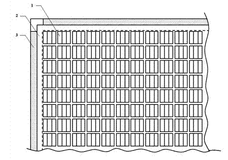
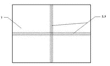
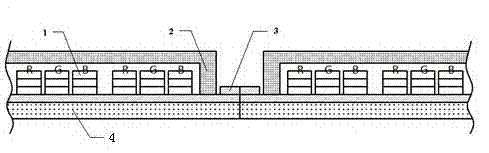
[0038] Such as Figure 4-7As shown, an OLED display module includes a substrate, an OLED structure for producing OLED light-emitting pixels, and an encapsulation layer for encapsulating the OLED structure. In the wiring area 6, contact wires 7 corresponding to the OLED light-emitting pixels are printed on the PCB substrate 5, and each contact wire 7 is connected to the OLED structure at the position of the corresponding OLED light-emitting pixel, and each contact wire 7 penetrates the PCB substrate 5 Connect to wiring area 6. In this embodiment, the PCB board is used as the substrate of the OLED display module, and the OLED light-emitting pixels are directly fabricated on the PCB substrate 5, and the contact wires 7 are circuit-wired on the PCB substrate 5 according to the distribution of the OLED display module light-emitting pixels, and The contact wire 7 leads through the PCB substrate 5 and is connected to the wiring area 6 on the back of the PCB substrate 5. By designing...

Embodiment 2

[0045] Such as Figure 10 As shown, the structure of Example 2 is similar to that of Example 1, the difference is that, in order to further reduce the non-luminous area of ​​the OLED display module, the OLED structure is sealed by thin-film packaging. Specifically, the encapsulation layer is a wetting thin film layer 8, and the wetting thin film layer 8 is distributed on the front, each side of the OLED structure and between each OLED light-emitting pixel. During production, the liquid monomer is evaporated to directly infiltrate the thin film onto the OLED light-emitting pixels, and condense to the surface of the device to form a layer of high molecular polymer film, that is, the infiltrating film layer 8 . The present invention does not need to retain the sealing area 2 when the wetting film layer 8 is used for encapsulation, and only the light emitting area 1 is reserved when viewed from the direction of the light emitting surface of the OLED display module.

[0046] Such ...

Embodiment 3

[0049] Such as Figure 13 As shown, the structure of embodiment 3 is similar to the structure of embodiment 1, the difference is that in order to reduce the OLED display module sealing area 2 and ensure the simplicity and feasibility of the process, the embodiment 3 uses a glass cover plate 10 clamp Encapsulation method of sealing glue. Specifically, the encapsulation layer includes a sealing glue layer 9 spin-coated on the OLED structure and a glass cover 10 disposed on the sealing glue layer 9 . During production, the sealing glue is spin-coated on the OLED structure, and the sealing glue completely infiltrates the light-emitting area 1 of the device to form a sealing glue layer 9, and then the glass cover plate 10 is directly pressed on the device coated with the sealing glue to complete the sealing process of the device . This encapsulation method ensures that there is no gap between the OLED structure, the sealing glue layer 9 and the glass cover 10 , and they are tight...


PUM


Abstract

The invention relates to the display technology of organic light emitting diodes, specifically to an OLED (organic light emitting diode) display module and an OLED spliced display screen with the OLED display module. The OLED display module comprises a substrate, an OLED structure used for generating OLED luminous pixels and a packaging layer used for packaging the OLED structure; and the substrate is a PCB (printed circuit board) substrate, wherein the OLED structure is arranged on the front side of the substrate, a wiring region connected with an external driving circuit is arranged on the back side of the substrate, contact wires corresponding to the OLED luminous pixels one by one are printed on the PCB substrate, and each of the contact wires is connected with the OLED structure at the position of the corresponding OLED luminous pixel, and is connected with the wiring region through the PCB substrate. According to the invention, a PCB is used as the substrate rather than a glass plate, and the existing non-luminous wiring region on the edge of the device is moved to the back side of the PCB substrate through leads of the contact wires, so that the non-luminous area of the device can be reduced, the splicing gap of the OLED spliced display screen spliced from the OLED display module can be greatly reduced, and the display effect of the screen can be well optimized.

Description

technical field [0001] The invention relates to an organic light emitting diode (OLED) display technology, in particular to an OLED display module and an OLED splicing display screen with the OLED display module. Background technique [0002] OLED is an organic light-emitting diode. It is a current-type light-emitting device based on organic materials. It has self-illumination, no backlight, all solid-state, ultra-thin, no viewing angle restrictions, fast response, wide operating temperature, and easy to realize flexible display. And 3D display and other advantages, is considered to be one of the most promising new FPD technologies. At present, the largest OLED screen that can be trial-produced is below 55 inches, and the OLED screens that are commercially put on the market are limited to 5-10 inches, and the size is small. Expensive raw materials. At present, splicing small-sized OLED display panels into large-sized display screens has great advantages in terms of technol...

Claims


Application Information

Patent Timeline
Patent Type & Authority Applications(China)
IPC IPC(8): H01L27/32H01L51/52G09F9/33
Inventor 彭晓林孙婷匡友元黄永峰
Owner GUANGDONG VTRON TECH CO LTD
Why Eureka
Try Eureka