

Method for growth of epitaxial layer of light emitting diode chip
A technology of light-emitting diodes and a growth method, which is applied in the field of epitaxial layer growth of light-emitting diode chips, can solve problems such as reducing the quality of light-emitting diode chips and affecting the internal quantum efficiency of light-emitting diode chips, so as to improve crystal quality and internal quantum efficiency, increase lateral Growth effect, effect of improving luminous efficiency
- Summary
- Abstract
- Description
- Claims
- Application Information
AI Technical Summary
Problems solved by technology
Method used
Image

Examples
Embodiment 1
[0025] An embodiment of the present invention provides a method for growing an epitaxial layer of a light emitting diode chip, the method comprising:
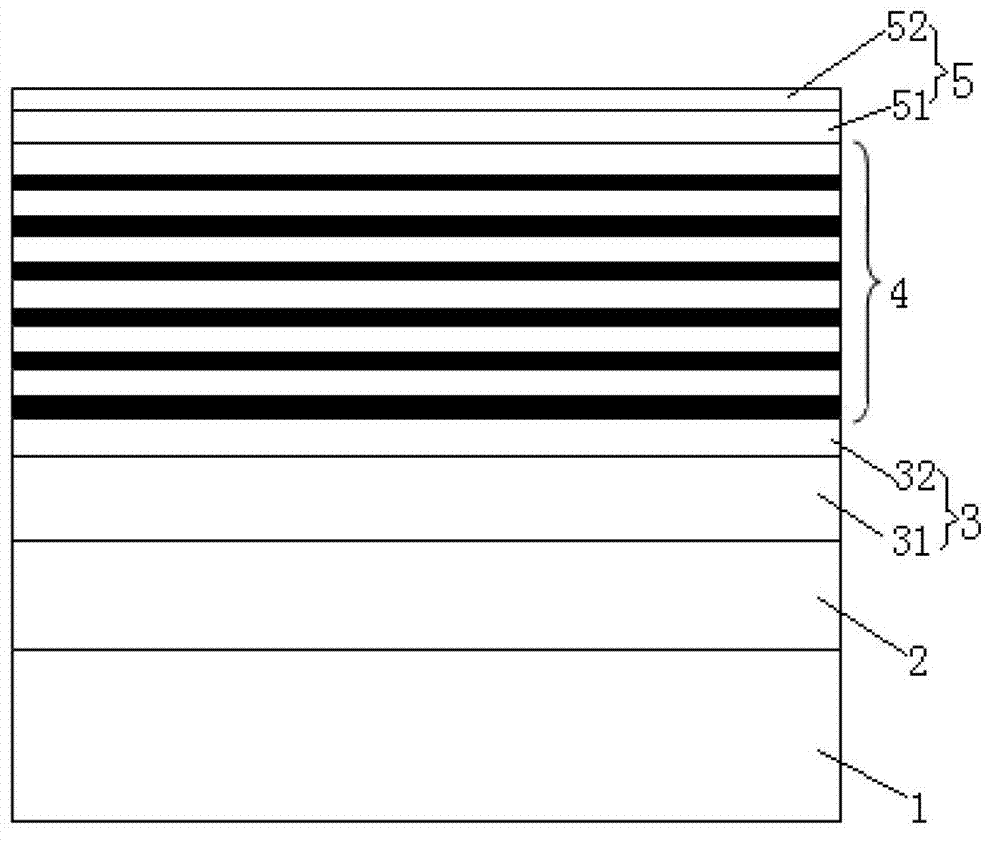
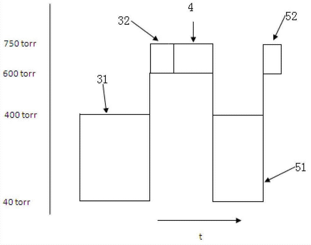
[0026] U-type GaN layer 2, n-type layer 3, quantum well active region layer 4, and p-type layer 5 are sequentially grown on substrate 1 by MOCVD method, such as figure 2 As shown, wherein, the growth pressure of the quantum active region layer 4 is 600-750 torr.
[0027] In specific implementation, this method can be realized through the following steps:
[0028] Step 101: Place the crystal-oriented sapphire substrate on a graphite disk and send it into the reaction chamber, heat the sapphire substrate to 1060° C. for 5 minutes.
[0029] Step 102: growing a 2um thick undoped GaN layer 2 under a low pressure of 200torr.
[0030] Step 103: growing a Si-doped n-type GaN carrier layer 31 with a thickness of 2 um under a low pressure of 40 torr.
[0031] Step 104: growing a Si-doped n-type GaN contact layer 32 with a thickness o...
Embodiment 2
[0038] An embodiment of the present invention provides a method for growing an epitaxial layer of a light emitting diode chip, see figure 2 , the method includes:
[0039] The MOCVD method is used to sequentially grow an undoped GaN layer 2, an n-type layer 3, a quantum well active region layer 4, and a p-type layer 5 on a substrate 1, such as figure 2 As shown, wherein, the growth pressure of the quantum active region layer 4 is 600-750 torr.
[0040] Preferably, the growth pressure of the n-type contact layer 32 is 600-750 torr.
[0041] Further, the growth pressure of the n-type GaN carrier layer 31 is 40-400 torr. In actual growth, in order to increase the growth speed, generally 40-400 torr is used to grow the n-type GaN carrier layer 31 . Apparently, the n-type GaN carrier layer 31 can also be grown with a high voltage of 600-750 torr, which can further increase the cracking effect of the material and reduce the defect density in the material.
[0042] It should be...
PUM
| Property | Measurement | Unit |
|---|---|---|
| Growth pressure | aaaaa | aaaaa |
| Growth pressure | aaaaa | aaaaa |
Abstract
Description
Claims
Application Information