

High-isolation double-unit MIMO (multiple input multiple output) antenna array
A high isolation, array antenna technology, applied in the field of MIMO antennas, to achieve the effect of simple implementation, good bandwidth characteristics, and improved isolation
- Summary
- Abstract
- Description
- Claims
- Application Information
AI Technical Summary
Problems solved by technology
Method used
Image

Examples
Embodiment Construction
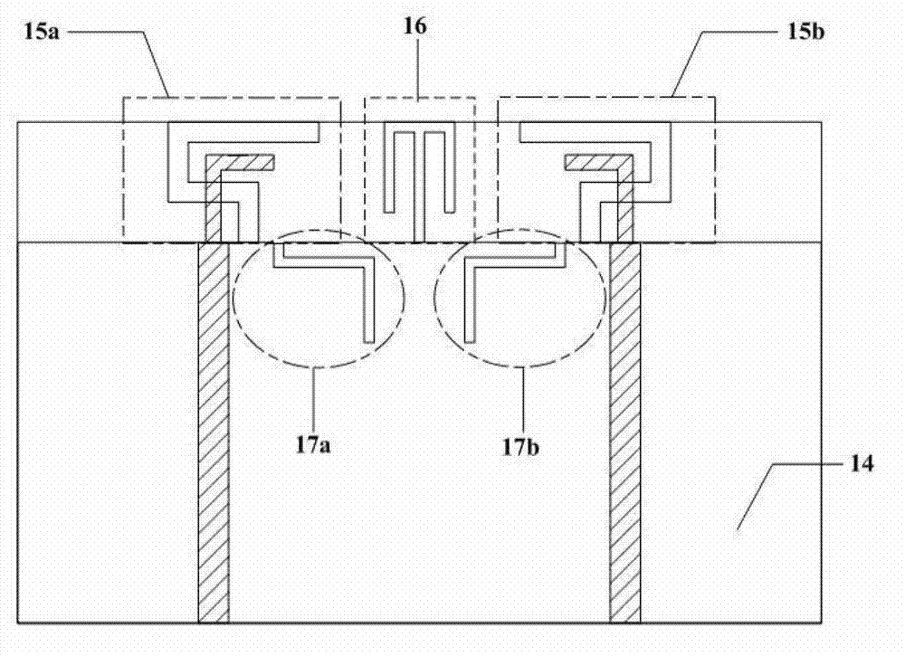
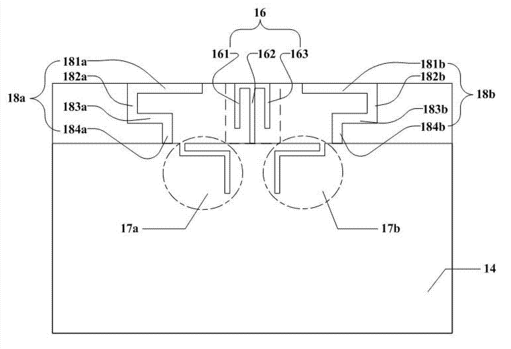
[0037]The present invention will be described in further detail below in conjunction with the accompanying drawings. Because there are 2 antenna elements in the present invention, that is, the first antenna element 15a and the second antenna element 15b; 2 isolation slots, that is, the first isolation slot 17a and the second isolation slot 17b; shape radiating unit 18a and the second type of C-shaped radiating unit 18b, and the first type of C-shaped radiating unit 18a includes a first branch 181a, a second branch 182a, a third branch 183a and a fourth branch 184a, and the second The C-like radiation unit 18b includes a first branch 181b, a second branch 182b, a third branch 183b and a fourth branch 184b; two inverted L-shaped radiation units are the first inverted L-shaped radiation unit 19a and the second inverted L-shaped radiation unit. The L-shaped radiation unit 19b, and the first inverted L-shaped radiation unit 19a includes a horizontal branch 191a and a vertical branc...
PUM
 Abstract
Description
Claims
Application Information