Liquid crystal device and manufacture method thereof

A technology of liquid crystal device and manufacturing method, which is applied in nonlinear optics, instruments, optics, etc., can solve the problems of high cost, large consumption of material resources, manpower and financial resources, etc., to improve adhesion, reduce production cost, increase humidity area effect

Active Publication Date: 2013-01-02
BOE TECH GRP CO LTD
View PDF9 Cites 16 Cited by
  • Summary
  • Abstract
  • Description
  • Claims
  • Application Information

AI Technical Summary

Problems solved by technology

[0005] Although the above solutions can achieve narrow borders, they all need to modify the materials, equipment or processes of the exis

Method used


Image

  • Liquid crystal device and manufacture method thereof
  • Liquid crystal device and manufacture method thereof
  • Liquid crystal device and manufacture method thereof

Examples


Embodiment 1

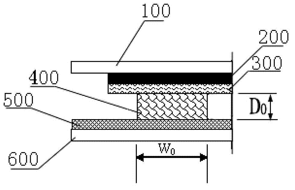
[0046] figure 2 is a schematic structural view of the liquid crystal device described in Embodiment 1 of the present invention, as figure 2 As shown, the liquid crystal device includes: a sealant 400, a protective film OC300, a black matrix layer BM200, and a color filter substrate 100 sequentially located above the sealant 400, and a protective layer PVX500 and Array substrate 600.

[0047] A first through hole is disposed on the protective film OC300 , and the first through hole penetrates through the protective film OC300 . A third groove is disposed on the black matrix layer BM200. The first through hole is arranged correspondingly to the third groove, has the same hole diameter and shape, and is connected as a whole. The upper part of the sealant 400 is located inside the first through hole and the third groove at the same time.

[0048] The protective layer PVX500 is provided with a second groove, and the lower part of the sealant 400 is located inside the second g...

Embodiment 2

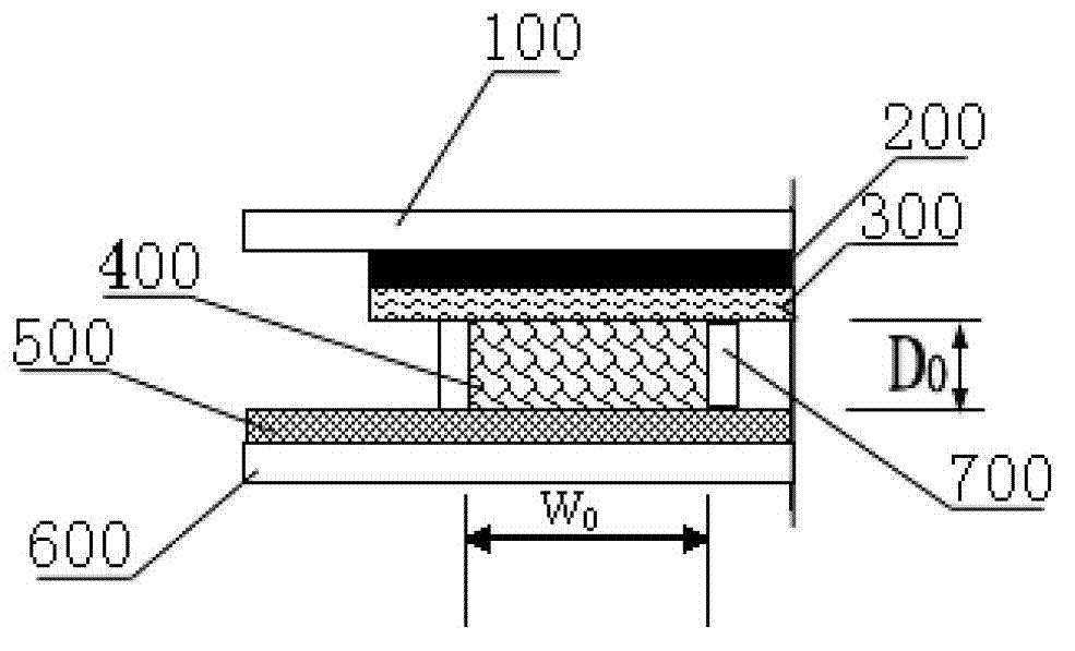
[0051] image 3 It is a structural schematic diagram of the liquid crystal device described in Embodiment 2 of the present invention, such as image 3 As shown, the liquid crystal device described in this embodiment is basically the same as the liquid crystal device described in Embodiment 1. The difference is that in this embodiment, only the first groove is provided on the protective film OC300, but not on the black matrix layer BM200. As for the third groove, the second groove is not provided on the protective layer PVX500. Wherein, the upper part of the sealant 400 is located inside the first groove, and the lower part is bonded to the protective layer PVX500. This design method can also increase the wet area of ​​the sealant 400, and its wet area increase value is W 0 ×d3, therefore, it is also possible to achieve a narrow border while ensuring the bonding effect of the liquid crystal device; at the same time, since the etching process of the black matrix layer BM200 an...

Embodiment 3

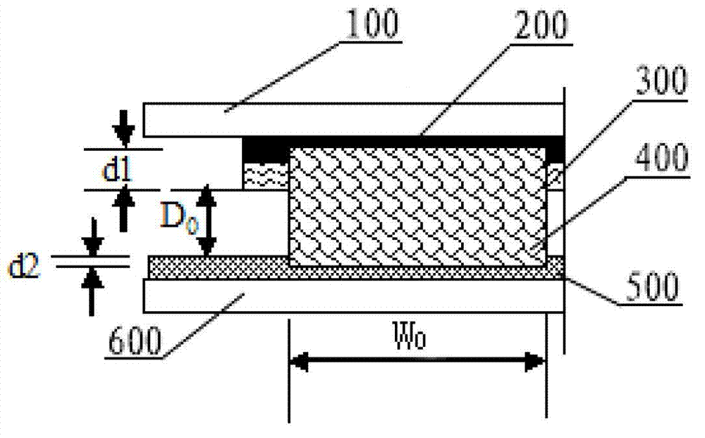
[0054] Figure 4 is a schematic structural view of the liquid crystal device described in Embodiment 3 of the present invention, as Figure 4 As shown, similar to Embodiment 2, the liquid crystal device described in this embodiment only has the second groove set on the protective layer PVX500, but does not set the third groove on the black matrix layer BM200, nor does it set the third groove on the protective film OC300. A slot or first through hole. This design method can also increase the wet area of ​​the sealant 400, and its wet area increase value is W 0 ×d4, therefore, a narrow frame can also be realized while ensuring the bonding effect of the liquid crystal device.

[0055] Wherein, when there is a via hole on the array substrate 600 , the depth d4 of the second groove cannot reach or exceed the thickness of the protection layer PVX500 , so as to prevent the electrodes on the array substrate 600 from being exposed.


PUM


Abstract

The invention discloses a liquid crystal device and relates to the field of liquid crystal display. The liquid crystal device comprises sealant, a protective film OC, a black matrix layer BM, a colored film substrate, a protective layer PVX and an array substrate, wherein the protective film OC, the black matrix layer BM and the colored film substrate are sequentially positioned above the sealant; the protective layer PVX and the array substrate are sequentially positioned below the sealant; a first groove or a first through hole is arranged above the protective film OC; the upper part of the sealant is positioned in the first groove or the first through hole; and/or, a second groove is arranged above the protective PVX, and the lower part of the sealant is positioned in the second groove. According to the liquid crystal device and the manufacture method, the hole or the groove is arranged on the upper structure (protective film OC and/or black matrix layer BM) or the lower structure (protective layer PVX) of the sealant, therefore, the height of a glue pouring space is increased, so that the wetted area of the sealant is increased, the binding power of the liquid crystal device is improved, and as a result, a narrow-side frame liquid crystal panel can be manufactured through common materials and equipment under common technologies, and the production cost is reduced.

Description

technical field [0001] The invention relates to the technical field of liquid crystal display, in particular to a liquid crystal device and a manufacturing method thereof. Background technique [0002] Narrow bezel is the latest concept in TV industrial design, which effectively increases the display area, realizes ultra-wide video screen, and provides convenience for applications such as multi-screen splicing. [0003] The frame of a narrow frame TV is generally only about half the width of the frame of an ordinary LCD TV. During the production process, the width of the sealant can be narrowed to achieve a narrow frame. At present, the main solutions to realize the narrowing of the frame are: the sealant manufacturer needs to improve the formula of the sealant to ensure that the sealant has a thin line characteristic, so that the narrow frame can be realized by reducing the amount of glue applied to the sealant under the premise of ensuring product quality; Optimize the pr...

Claims


Application Information

Patent Timeline
IPC IPC(8): G02F1/1339G02F1/1333G02F1/1335
Inventor 黄华
Owner BOE TECH GRP CO LTD
Why Eureka
Try Eureka