
Eureka
For R&D, Eureka makes reading and utilizing patents & technical documents easy.
Eureka AIR
Designed for self-driven R&D workflows. Generate viable solutions, solve complex R&D challenges, empower your innovation with AI.

Eureka Materials
Designed for material experts only. Revolutionize your material R&D, from search, analyze, to developing new materials.

TechResearch
Generate reliable direction feasibility study reports for your R&D in just a few steps.

TechSeek
Discover and master advanced knowledge NOW. Basics, ideas, possibilities, all at once.

TechMind
As an expert in R&D Theories, TechMind can generates customized viable solutions instantly.

TechRisk
Analyze your overall solution with one click, know your potential R&D risks in advance.

TechMonitor
Get weekly tech updates, stay abreast of the latest tech innovations and key insights.
Electronic equipment and power management circuit
A technology of electronic equipment and power management, which is applied in the electronic field, can solve the problems of electronic equipment consumption of electric energy, the inability to use normally open button switches, and the inability to input other signals with electronic equipment, so as to achieve the effect of saving electric energy consumption
- Summary
- Abstract
- Description
- Claims
- Application Information
AI Technical Summary
Problems solved by technology
Method used
Image

Examples
Embodiment 1
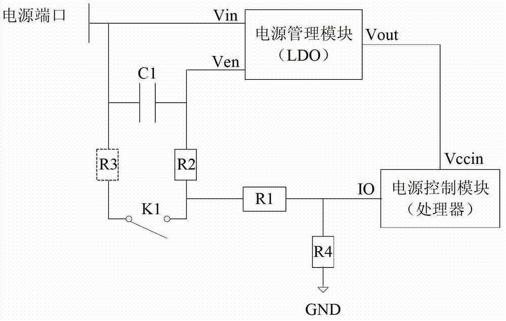
[0039] figure 1 It is a schematic structural diagram of the first embodiment of the electronic device including the power management circuit of the present invention; as figure 1 As shown, the electronic device includes: a power port, a power management module, a power control module, a capacitor C1, and a switch K1; in addition, the electronic device may also include resistors R1-R4; wherein:
[0040] The power port is used to output power, for example, the power port can be the VBUS pin of the USB interface, which outputs 5V power.
[0041] The power management module is coupled with the power port, and outputs or stops outputting power according to the power management control signal after receiving the power management control signal.
[0042] It is worth noting that coupling includes direct connection and indirect connection (including coupling connection). Direct connection refers to the direct contact between the two connected parties. Or the circuit is connected indi...
Embodiment 2
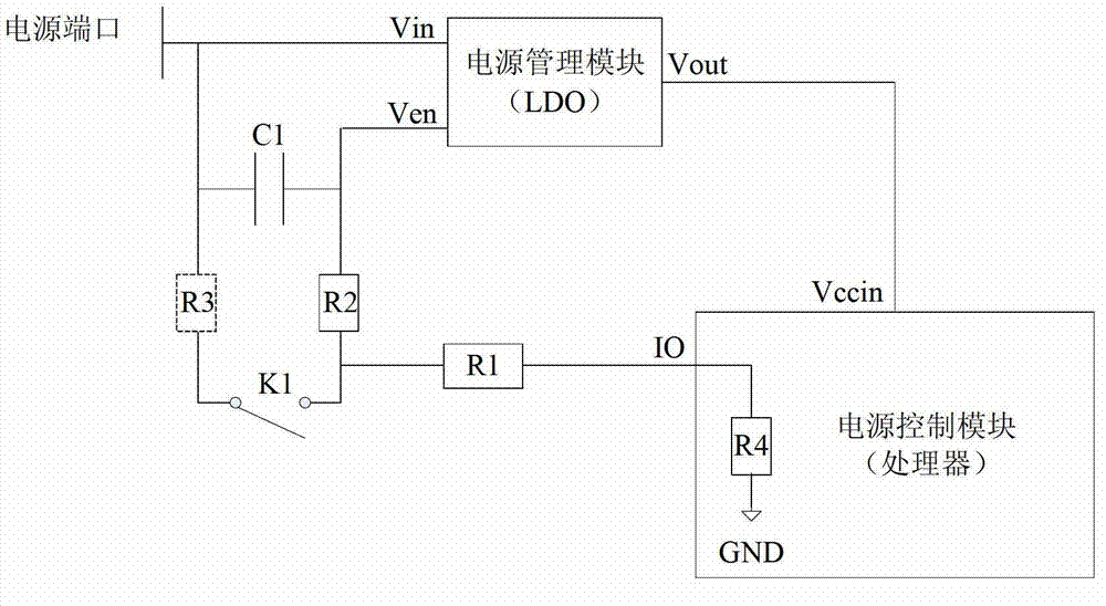
[0072] figure 2 It is a schematic structural diagram of the second embodiment of the electronic device including the power management circuit of the present invention; as figure 2 As shown, the difference between the second embodiment of the present invention and the first embodiment is only that the external pull-down resistor in the first embodiment is changed to the built-in pull-down resistor of the power control module (processor).
Embodiment 3
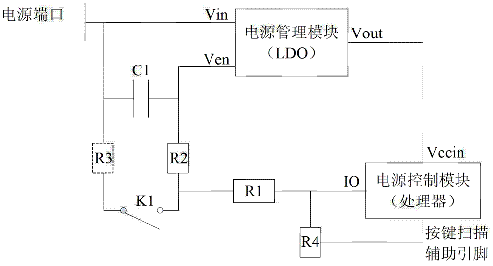
[0074] image 3 It is a schematic structural diagram of the third embodiment of the electronic device including the power management circuit of the present invention; as image 3 As shown, compared with the first embodiment, the third embodiment of the present invention differs in that:
[0075] One end of the resistor R4 is coupled to the IO pin of the power control module, and the other end is coupled to the output pin (which may be called a key scanning auxiliary pin) of the power control module.
[0076] When the power control module / processor performs key scanning and enters the key scanning state, in addition to setting its IO pins to the input state, it also outputs a low level through the key scanning auxiliary pin (for example, the voltage is lower than or equal to 0.3V Level).
[0077] In this embodiment, it is assumed that the key scanning auxiliary pin outputs a level of Vl=0.3V; when the switch K1 is in the closed state, the level voltage of the IO input of the ...
PUM
 Abstract
Description
Claims
Application Information
 - R&D Engineer
- R&D Manager
- IP Professional
- Industry Leading Data Capabilities
- Powerful AI technology
- Patent DNA Extraction
Browse by: Latest US Patents, China's latest patents, Technical Efficacy Thesaurus, Application Domain, Technology Topic, Popular Technical Reports.
© 2024 PatSnap. All rights reserved.Legal|Privacy policy|Modern Slavery Act Transparency Statement|Sitemap|About US| Contact US: help@patsnap.com