Manufacture method for active layer of carbon nano tube field effect transistor

A field effect transistor and carbon nanotube technology, which is applied in the fields of nanotechnology, nanotechnology, semiconductor/solid-state device manufacturing, etc., can solve the problems of extremely demanding physical and chemical properties of ink, easy aggregation of carbon nanotubes, and high cost of printing equipment , to achieve the effect of good transmission characteristics, low cost, and simplified production methods

Inactive Publication Date: 2013-01-02
SUZHOU INST OF NANO TECH & NANO BIONICS CHINESE ACEDEMY OF SCI
View PDF3 Cites 7 Cited by
  • Summary
  • Abstract
  • Description
  • Claims
  • Application Information

AI Technical Summary

Benefits of technology

This patented describes methods for making small devices with excellent electrical properties by creating layers made from carbon materials called CNT's or graphene tubules on top of another material like silicon dioxide (SiO2). These techniques allow for better control over their conductive behavior during operation compared to traditional ways involving lithography processes. Additionally, this technique allows for easy fabrications without requiring special equipment while also providing strength against environmental factors like moisture and air. Overall, these technical results improve the efficiency and quality of producing highly functional electronics.

Problems solved by technology

Technological Problem addressed by this patented technical issue relates to improving the production efficiency and purification of 2D networks made from carbon nanostructures like graphene or fullerenic tubules. Current methods involve expensive processes involving vacuum deposition techniques, solvent evaporation technique, spray painting, lithography, etc., making them difficult to scale up into industrial applications due to these challengings.

Method used


Image

  • Manufacture method for active layer of carbon nano tube field effect transistor
  • Manufacture method for active layer of carbon nano tube field effect transistor
  • Manufacture method for active layer of carbon nano tube field effect transistor

Examples


Embodiment 1

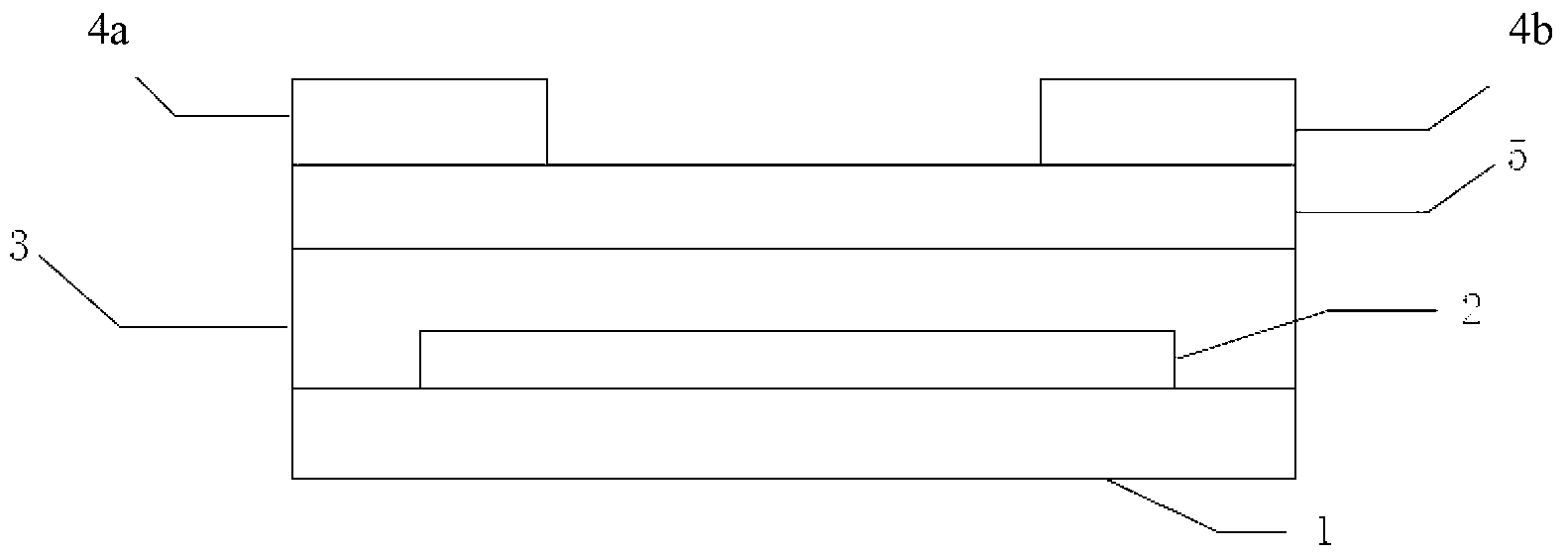
[0024] In this embodiment, a bottom gate-top contact type carbon nanotube field effect transistor is taken as an example. Such as figure 1 As shown, the carbon nanotube field-effect transistor is composed of substrate 1, gate 2, insulating layer 3, active layer 5, source 4a, and drain 4b from bottom to top. Wherein, the preparation method of the active layer 5 is as follows:

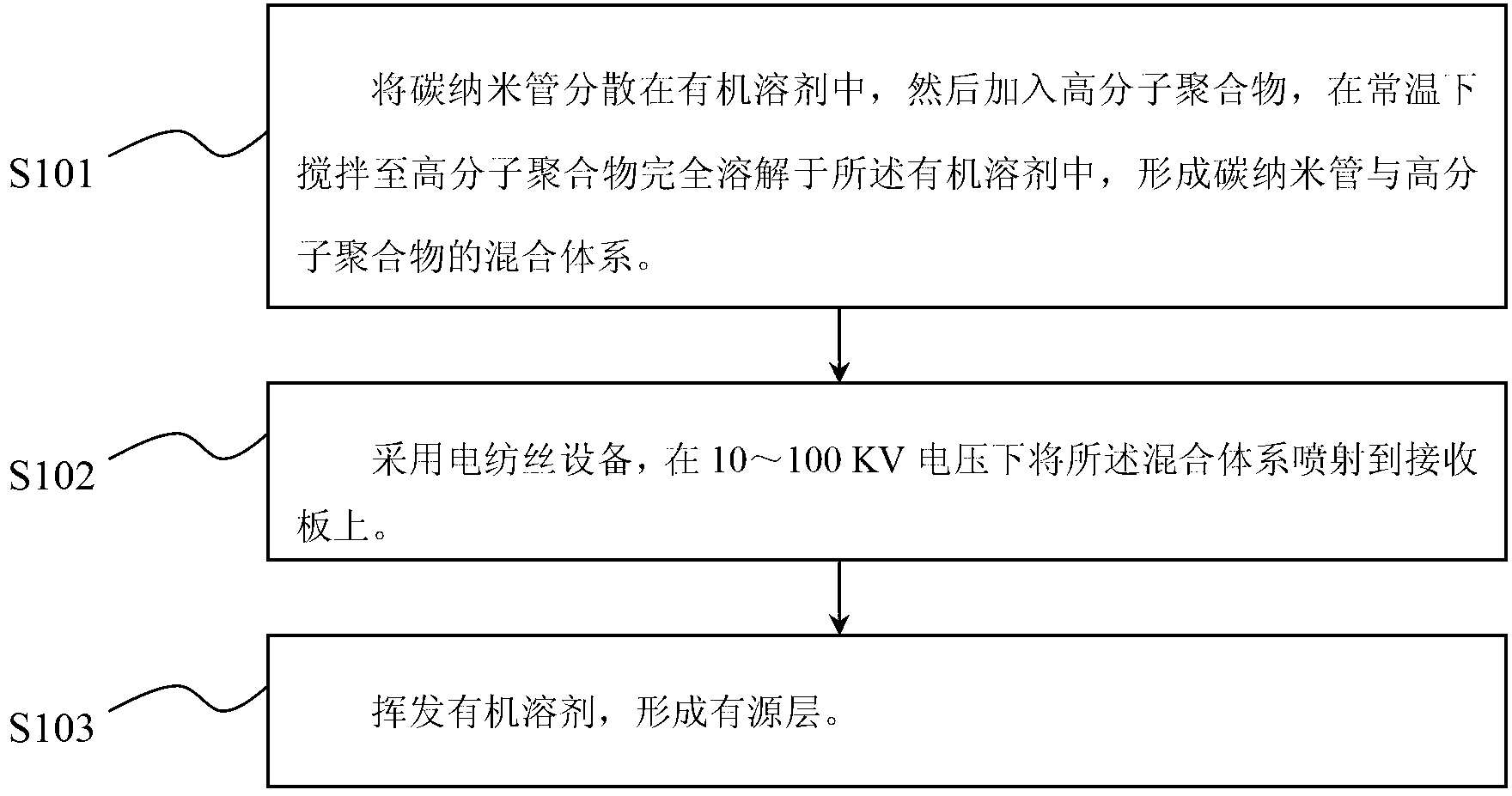
[0025] In this embodiment, carbon nanotubes (hereinafter referred to as CNT) are used as raw materials, chloroform is used as an organic solvent, and the high molecular polymer is polyacrylonitrile. Combine figure 2 Steps S101 to S103 in step S101, the manufacturing process of the active layer in this embodiment: First, CNTs are dispersed in chloroform by vigorous stirring for 2h, and then polyacrylonitrile is added in a ratio of 1:1 to the mass ratio of CNTs. Stir with a magnetic stirrer for 0.5 h at °C until the polyacrylonitrile is completely dissolved in the chloroform to form a CNT and polyacrylonitr...

Embodiment 2

[0031] In this embodiment, a top gate-top contact type CNT field effect transistor is fabricated, such as Figure 4 Shown. The CNT field effect crystal structure of this embodiment is: from bottom to top, the substrate 1, the active layer 5, the source 4a and the drain 4b, the insulating layer 3, and the gate 2 in order.

[0032] Wherein, in the manufacturing steps of the active layer 5 in this embodiment, the high molecular polymer adopts polyvinyl alcohol, and the mass ratio of CNT to CNT is 1:4, and the mass concentration after being dissolved in ethanol to form a mixed system is 10wt%. Then, through a spinneret with an inner diameter of 5 mm, a voltage of 100 KV was applied, and the mixed system was sprayed onto a receiving plate (ie, substrate 1) 30 cm from the nozzle of the spinneret. For the remaining steps of the method for preparing the active layer 5, reference may be made to Embodiment 1. Further, the substrate 1 of this embodiment is ceramic, and the source electrode...

Embodiment 3

[0034] In this embodiment, a top gate-bottom contact type CNT field effect transistor is fabricated, such as Figure 5 Shown. The CNT field effect crystal structure of this embodiment is: from bottom to top, the substrate 1, the source 4a and the drain 4b, the active layer 5, the insulating layer 3, and the gate 2 in order.

[0035] Wherein, in the manufacturing steps of the active layer 5 in this embodiment, the high molecular polymer is polystyrene, and the mass ratio of the CNT is 1:10, and the mass concentration after being dissolved in toluene to form a mixed system is 15 wt%. Then through the spinneret with the inner diameter of the tube head of 1mm, apply a voltage of 20KV, and spray the mixed system to the receiving plate 10cm away from the spinneret tube head (ie the source 4a, the drain 4b and the substrate between them). 1) On the surface. For the remaining steps of the method for preparing the active layer 5, reference may be made to Embodiment 1. Further, the subst...


PUM


Abstract

The invention relates to the technology of semi-conductors and provides a manufacture method for an active layer of a carbon nano tube field effect transistor. The manufacture method includes the following steps: dispersing carbon nano tubes in organic solvents, adding high-molecular polymer, stirring at room temperature to enable the high-molecular polymer to fully dissolve in the organic solvents so as to form a mixed system of the carbon nano tubes and the high-molecular polymer, and ejecting the mixed system onto a receiving board at the voltage of 10-100 KV by adopting an electronic spinning device; and enabling the organic solvents to volatilize so as to form the active layer. The method for manufacturing the carbon nano tube field effect transistor has the advantages of being low in cost, small in requirements for the environment and easy in manufacture technology, the obtained organic electronic devices have strong water oxidizing resisting performance, the method for manufacturing the active layer is well simplified, and performance of the active layer is improved simultaneously.

Description


Claims


Application Information

Patent Timeline
Owner SUZHOU INST OF NANO TECH & NANO BIONICS CHINESE ACEDEMY OF SCI
Why Eureka
Try Eureka