Silicon-based uniwafer photoelectricity integrated receiving chip for plastic optical fiber communication

A technology of optical fiber communication and optoelectronic integration, applied in optical fiber transmission, circuits, electrical components, etc., to achieve the effect of reducing cost, increasing bandwidth, and reducing junction capacitance

Active Publication Date: 2013-01-02
XIAMEN UNIV
View PDF4 Cites 13 Cited by
  • Summary
  • Abstract
  • Description
  • Claims
  • Application Information

AI Technical Summary

Problems solved by technology

However, the BCD standard process can integrate Bipolar devices, CMOS devices and DMOS devices on the same substrate, which combines the advantages of high transconductance, strong load driving capability of bipolar devices, high integration and low power consumption of CMOS, and can also become a An innovative idea and be

Method used


Image

  • Silicon-based uniwafer photoelectricity integrated receiving chip for plastic optical fiber communication
  • Silicon-based uniwafer photoelectricity integrated receiving chip for plastic optical fiber communication
  • Silicon-based uniwafer photoelectricity integrated receiving chip for plastic optical fiber communication

Examples


Embodiment Construction

[0030] The silicon-based monolithic optoelectronic integrated receiving chip described in the embodiment of the present invention is prepared by a 0.5 μm standard BCD process, and is equipped with a silicon-based photodetector and a preamplifier integrated circuit.

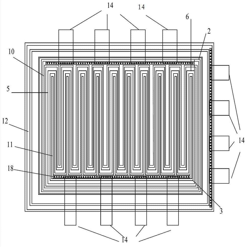
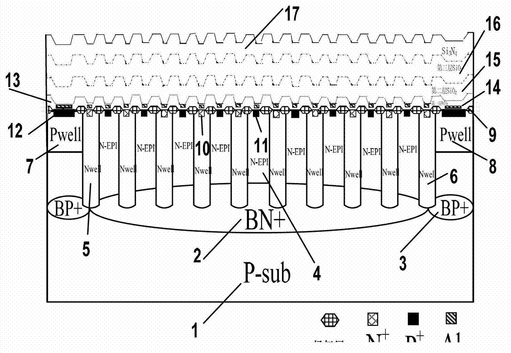
[0031] see figure 1 with 2 , the structure of the silicon-based photodetector and its manufacturing process are described as follows: First, the BN+ buried layer region is photolithographically etched on the high-resistance P-type silicon substrate 1, and the BN+ buried layer 2 and BP+ buried layer 2 are formed by ion implantation. Buried layer 3. N-EPI epitaxial layer 4 is grown on BN+buried layer 2 and BP+buried layer 3 . On the epitaxial layer 4, there are 11 N well regions with a distance of 14.6 μm and a width of 6.3 μm on the photolithography at equal intervals, and the 11 N wells are realized by ion implantation technology. Lithograph the P well area around the N wells 5 and 6, and use ion implantation ...


PUM

PropertyMeasurementUnit
Horizontal sizeaaaaaaaaaa
Lengthaaaaaaaaaa

Abstract

The invention discloses a silicon-based uniwafer photoelectricity integrated receiving chip for plastic optical fiber communication, and relates to a silicon-based uniwafer photoelectricity integrated circuit. The chip is a uniwafer photoelectricity integrated receiving chip with the wavelength of 650 +/- 17.8nm for the plastic optical fiber communication; and a photoelectricity probe chip and a preposed amplifying integrated circuit chip in a light receiving module with the wavelength of 650 +/- 17.8nm for the conventional plastic optical fiber communication can be replaced by the chip, so that the uniwafer photoelectricity integration of the photoelectricity probe and the preposed amplifying integrated circuit with the wavelength of 650 +/- 17.8nm is realized; a requirement on 100Mbps transmission velocity for the plastic optical communication can be met; and the chip can be used for the light receiving end with the wavelength of 650 +/- 17.8nm for the plastic optical fiber communication; and moreover, the chip can be prepared by a 0.5-micron standard binary-coded decimal (BCD).

Description

technical field [0001] The invention relates to a silicon-based single-chip photoelectric integrated circuit, in particular to a silicon-based single-chip photoelectric integrated receiving chip for plastic optical fiber communication. Background technique [0002] Plastic optical fiber communication is a new generation of short-distance transmission system. It has the advantages of simplicity, high speed, low cost, and flexible and bendable optical fiber. It can successfully solve the "last 100 meters" access problem in optical fiber communication and replace the existing copper cables. Realize fiber-to-the-desktop all-optical network communication. The development of plastic optical fiber communication not only conforms to the development strategy of optical fiber broadband to the home and "optical into copper" in the national "Twelfth Five-Year Plan", but also plays an important role in promoting the integration of three networks, smart home networks, industrial control, ...

Claims


Application Information

Patent Timeline
IPC IPC(8): H01L27/06H01L31/0352H01L31/105H04B10/25
Inventor 程翔史晓凤李继芳陈朝潘江炳颜黄苹卞剑涛
Owner XIAMEN UNIV
Why Eureka
Try Eureka