Silicon-based photoelectric detector for photoelectric monolithic integration and preparation method thereof

A photodetector and monolithic integration technology, which is applied in semiconductor/solid-state device manufacturing, circuits, electrical components, etc., can solve problems such as low frequency response, poor short-wave response, and incomplete compatibility between preparation technology and standard technology, and achieve good results. Isolation effect, compatibility of preparation process, and the effect of overcoming poor short-wave response

Active Publication Date: 2010-06-02
XIAMEN UNIV
View PDF0 Cites 14 Cited by
  • Summary
  • Abstract
  • Description
  • Claims
  • Application Information

AI Technical Summary

Problems solved by technology

[0009] The purpose of the present invention is to provide a kind of photoelectric monolithic photodetector that is fully compatible with the commercial BCD standard process in view of the shortcomings of the existing silicon-based photodetectors, such as poor short-wave response, low frequency response, and incomplete compatibility between the preparation process and the standard process. Chip-integrated silicon-based photodetectors and fabrication methods thereof

Method used


Image

  • Silicon-based photoelectric detector for photoelectric monolithic integration and preparation method thereof
  • Silicon-based photoelectric detector for photoelectric monolithic integration and preparation method thereof
  • Silicon-based photoelectric detector for photoelectric monolithic integration and preparation method thereof

Examples


Embodiment Construction

[0054] The following embodiments will further illustrate the present invention in conjunction with the accompanying drawings.

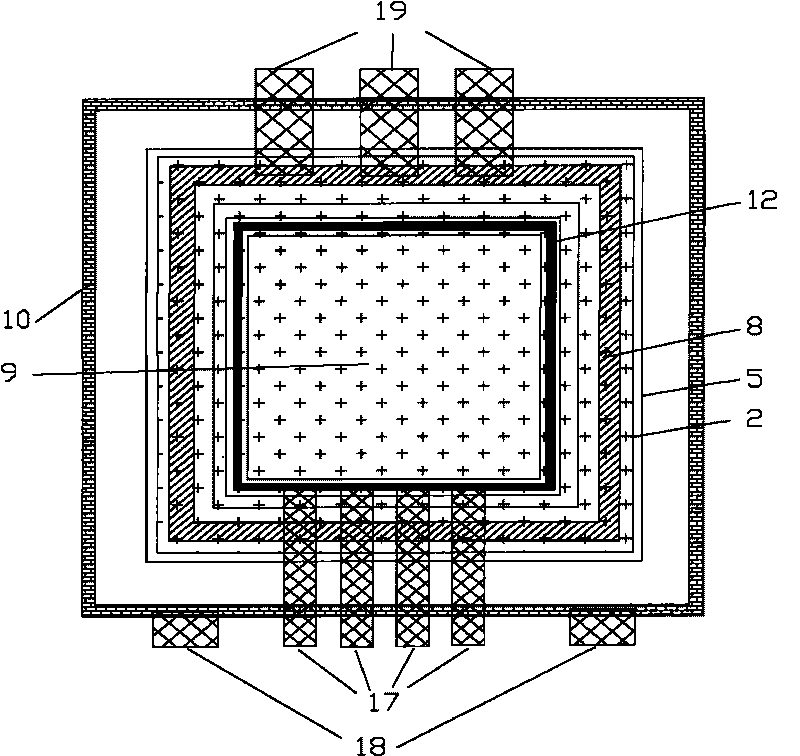
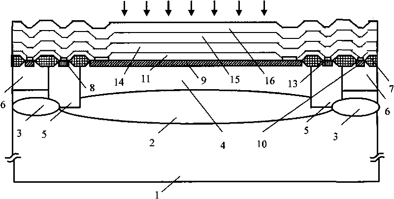
[0055] figure 1 and figure 2 The manufacturing process flow of the silicon-based photodetector under the BCD standard process shown is as follows: first, BN is photolithographically etched on a P-type silicon substrate 1 with a resistivity of 15-25Ωcm. + The buried layer region, and the implantation dose is about 1×10 by ion implantation process 15 Antimony forms BN + Buried layer 2. The implantation dose by ion implantation process is about 4×10 12 The boron forms BP + Buried layer 3. in BN + Buried layer 2 and BP + An N-EPI epitaxial layer 4 is grown on the buried layer 3 . The resistivity of the N-EPI epitaxial layer 4 is 3.5 Ωcm, and the thickness is 4.5 μm. The N well region is photolithographically etched on the epitaxial layer 4, and the implantation dose is about 6.5×10 by ion implantation process. 12 Phosphorus is used to realize...


PUM


Abstract

The invention discloses a silicon-based photoelectric detector for photoelectric monolithic integration and a preparation method thereof, which relates to a silicon-based photoelectric monolithic integrated circuit. The invention provides the silicon-based photoelectric detector which is completely compatible with the commercial BCD standard technology and is used for photoelectric monolithic integration, and provides the preparation method thereof. The silicon-based photoelectric detector is provided with a P type silicon substrate, a BN+ epitaxial layer, a BP+ epitaxial layer, an N-EPI epitaxial layer, an N-well layer, a P-well layer, a P+ layer, an N+ layer, an Al layer, a field oxide layer, SiO2 insulating medium layers and a Si3N4 surface passivation layer, wherein the P type silicon substrate, the BN+ epitaxial layer, the BP+ epitaxial layer, the N-EPI epitaxial layer, the N-well layer, the P-well layer, the P+ layer and the N+ layer are arranged on the same silicon wafer; the field oxide layer is a silicon oxide layer generated on the surface of the silicon wafer; a metallic aluminum layer is deposited on the surface of the silicon wafer; three SiO2 insulating medium layers are attached to the silicon substrate from bottom to top according to the preparation sequence through the deposition technology; and the Si3N4 surface passivation layer is attached to the SiO2 insulating medium layers through the deposition technology.

Description

technical field [0001] The invention relates to a silicon-based photoelectric single-chip integrated circuit, in particular to a silicon-based photodetector for photoelectric monolithic integration and a preparation method thereof which is fully compatible with the BCD standard process. Background technique [0002] The function of the photodetector is to efficiently convert the input optical signal into an electrical signal. In recent years, silicon-based photodetectors have developed rapidly and are widely used in optical storage systems, photoelectric measurement, optical data transmission and optical interconnection, optical computing, and image storage and processing. For example, silicon-based photodetectors can be applied to optical pickup heads of CD-ROM, digital video disc (DVD), etc., as well as 850nm optical fiber communication and 650nm plastic optical fiber communication. [0003] Taking the 850nm light receiving chip as an example, the light receiving chip is ...

Claims


Application Information

Patent Timeline
Patent Type & Authority Applications(China)
IPC IPC(8): H01L27/144H01L31/08H01L21/822H01L31/18
CPCY02P70/50
Inventor 颜黄苹程翔卞剑涛陈朝芦晶
Owner XIAMEN UNIV
Why Eureka
Try Eureka