PCB (printed circuit board), laminating method for PCB and COF (chip on FPC (flexible printed circuit)), as well as liquid crystal display device

A liquid crystal display device, printed circuit board technology, applied in the structural connection of printed circuits, printed circuits, printed circuits, etc., can solve problems such as difficulty, failure to use normally, defective products, etc., to reduce deformation accumulation and improve connection accuracy sexual effect

Inactive Publication Date: 2013-01-02
SHENZHEN CHINA STAR OPTOELECTRONICS TECH CO LTD
View PDF2 Cites 6 Cited by
  • Summary
  • Abstract
  • Description
  • Claims
  • Application Information

AI Technical Summary

Problems solved by technology

However, the longer the PCBA board, the greater the expansion, and the expansion and deformation accumulated on both sides will cause a large offset in the pressing area 102, and the contact between the pressing area 102 and the flexible circuit board 200 will be offset, resulting in ineffective connection.
like image 3 As shown, before lamination, the left, middle, and right of the entire flexible circuit board 200 are aligned on the golden fingers 103 of the lamination area 102 of the printed circuit board assembly 100, as shown in Figure 4 As shown, after lamination, due to the expansion of the PCBA, the overall expansion will be added to the lamination area 102 so that the gold fingers 103 in the lamination area 102 and the traces 201 on the left, middle, and upper right of the entire flexible circuit board 200 will have a relatively large gap. A large misalignment will affect the connectivity, and may even break the circuit and cause the product to fail to work normally
The current way to overcome it will be to shrink the design in advance and control the temperature of the same equipment to overcome it. However, it will be difficult to design or control the equipment, and it will take multiple experiments to obtain reasonable conditions and design values. And poor regulation will lead to the occurrence of bad products

Method used


Image

  • PCB (printed circuit board), laminating method for PCB and COF (chip on FPC (flexible printed circuit)), as well as liquid crystal display device
  • PCB (printed circuit board), laminating method for PCB and COF (chip on FPC (flexible printed circuit)), as well as liquid crystal display device
  • PCB (printed circuit board), laminating method for PCB and COF (chip on FPC (flexible printed circuit)), as well as liquid crystal display device

Examples


Embodiment 1

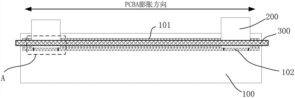
[0032] Such as Figure 5-Figure 9 As shown, the method for connecting the printed circuit board assembly 100 (PCBA) and the flexible circuit board 200 (COF) includes steps:

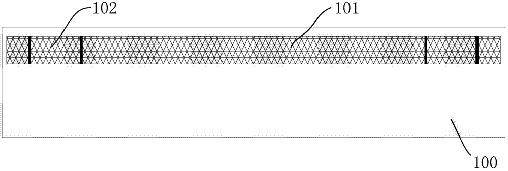
[0033] A. If Figure 5 As shown, avoidance grooves 120 are provided on one side or both sides of the pressing area 102 between the printed circuit board assembly 100 and the flexible circuit board 200 .

[0034] B. If Figure 6 As shown, the flexible circuit board 200 is bonded to the printed circuit board assembly 100 by using a high temperature bonding cutter head 300 so that the two are connected to the bonding area 102 .

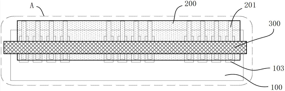
[0035] In this embodiment, two pressing areas 102 are provided on the driving printed circuit board assembly 100 of the liquid crystal display device, and only one space-avoiding groove 120 is provided between two adjacent pressing-bonding areas, and the space-avoiding groove 120 It starts from the boundary of one pressing area 102 and ends at the boundary of another pressing are...

Embodiment 2

[0039] Such as Figure 10 As shown, the difference from the first embodiment is that two space-avoiding grooves 120 are provided between the two pressing areas 102, and the printed circuit board sheet is still reserved between the two space-avoiding grooves 120, so that the printed circuit board can be enlarged. In this way, the deformation of the printed circuit board sheet retained between the two avoidance grooves 120 can be prevented from accumulating to the pressing area 102 when it expands. The avoidance grooves 120 between the two press-fit regions 102 are all arranged on one side of the press-fit regions 102, and the other side of the press-fit regions 102 is also provided with the avoidance grooves 120, that is to say, each press-fit region 102 Evacuation grooves are provided on both sides of the two sides, and each relief groove 120 is terminated at the boundary of the adjacent pressing area 102 .

[0040] Such as Figure 11 As shown, although the reserved part is ...


PUM


Abstract

The invention discloses a PCB (printed circuit board), a connecting method for the PCB and a COF (chip on FPC (flexible printed circuit)), as well as a liquid crystal display device. The connecting method comprises the following steps: A, a clearance groove/clearance grooves is/are arranged at one side or two sides of a laminating area/laminating areas of the PCB, wherein the PCB and the COF are laminated on the laminating area/laminating areas; B, a high-temperature laminating cutter bit is used for laminating the COF and the printed circuit board assembly (PCBA), so that the COF and the PCBA are connected on the laminating area/laminating areas. According to the invention, as the clearance grooves are arranged at the two sides of the laminating areas at which the PCBA and the COF are laminated, so that the two sides of the laminating area/laminating areas of the PCBA are not affected by the high temperature of the laminating cutter bit, thereby avoiding the defect that the distortion of the PCB at the two sides is accumulated on the PCB on the laminating area/laminating areas so that large displacement of golden fingers on the laminating area/laminating areas can be caused and ensuring the connection accuracy of a leading wire of the COF and the golden fingers on the PCBA.

Description

technical field [0001] The invention relates to the field of liquid crystal display devices and manufacturing, more specifically, to a printed circuit board, a method for laminating it with a flexible circuit board, and a liquid crystal display device. Background technique [0002] In today's liquid crystal display manufacturing process, it often involves the interconnection between the flexible circuit board (COF, Chip on FPC) and the printed circuit board (PCB), and the interconnection between the display electrode and the flexible circuit. In these connections, the anisotropic conductive film is widely used, placed between the parts to be connected, and then pressurized and heated to form a stable and reliable mechanical and electrical connection between the parts. [0003] figure 1 Shown is a schematic diagram of a current liquid crystal display driver printed circuit board assembly (PCBA) 100 . The printed circuit board assembly 100 is provided with a golden finger ar...

Claims


Application Information

Patent Timeline
Patent Type & Authority Applications(China)
IPC IPC(8): H05K3/36H05K1/14G02F1/13
CPCG02F1/13452H05K3/361H05K2201/10136
Inventor 郭东胜朱江
Owner SHENZHEN CHINA STAR OPTOELECTRONICS TECH CO LTD
Why Eureka
Try Eureka