Driving circuit of liquid crystal panel

A driving circuit and liquid crystal panel technology, applied in nonlinear optics, instruments, optics, etc., can solve problems such as increasing the deflection state time of liquid crystal molecules, liquid crystal molecule deflection, abnormal ratio display, etc., to reduce abnormal conduction The possibility of reducing the conduction time and improving the accuracy

Active Publication Date: 2013-01-16
CHANGSHA HKC OPTOELECTRONICS CO LTD
View PDF5 Cites 5 Cited by
  • Summary
  • Abstract
  • Description
  • Claims
  • Application Information

AI Technical Summary

Problems solved by technology

Such an effect appears at the drain D side as V d The voltage drift of (N, j) increases the time that the liquid crystal molecules are in the d

Method used


Image

  • Driving circuit of liquid crystal panel
  • Driving circuit of liquid crystal panel
  • Driving circuit of liquid crystal panel

Examples


Embodiment Construction

[0026] In order to further illustrate the technical means adopted by the present invention and its effects, the following describes in detail in conjunction with preferred embodiments of the present invention and accompanying drawings.

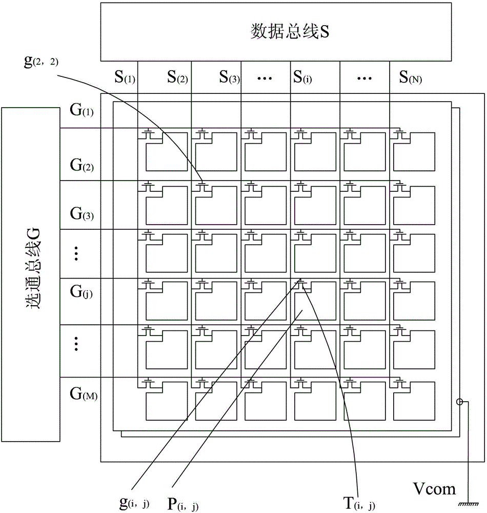
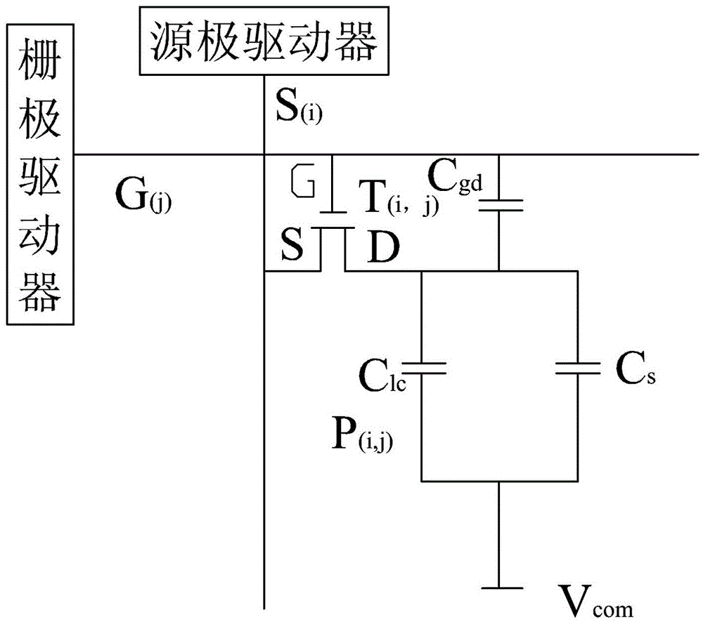
[0027] see Figures 4 to 6 , the present invention provides a driving circuit for a liquid crystal panel, comprising: a gate driver 2, a source driver 4, a plurality of gate lines G(j) and a plurality of data lines S(i), the plurality of gate lines G (j) and the data line S(i) define a plurality of pixel units, each pixel unit includes a thin film transistor T (i, j), a common electrode 8, a thin film transistor T (i, j) electrically connected Pixel electrode 6, and a correction capacitor C 0 , the thin film transistor T(i, j) is electrically connected to the gate driver 2 and the source driver 4 respectively through the gate line G(j) and the data line S(i), and the common electrode 8 is connected to the pixel electrode 6 form a liquid crys...


PUM


Abstract

The invention provides a driving circuit of a liquid crystal panel. The driving circuit comprises a gate driver, a source driver, a plurality of gating lines and a plurality of data lines, wherein a plurality of pixel units are defined by the gating lines and the data lines; each pixel unit comprises a thin film transistor, a public electrode, a pixel electrode and a correction capacitor; the thin film transistor is electrically connected with the gate driver and the source driver through one gating line and one data line respectively; the public electrode and the pixel electrode form a liquid crystal capacitor; the thin film transistor comprises a gate and a drain; and the correction capacitor is electrically connected between the gate and the drain for correcting parasitic capacitance formed by the gate and the drain due to structural characteristic. The influence of the parasitic capacitance on the thin film transistor is reduced by arranging the correction capacitor, so that the accuracy in control of the thin film transistor is improved, and phenomena of variation in transmittance and contrast abnormality caused by abnormal deflection of liquid crystal molecules are avoided.

Description

technical field [0001] The invention relates to the field of liquid crystal displays, in particular to a driving circuit of a liquid crystal panel. Background technique [0002] With the development of science and technology and the improvement of people's quality of life, liquid crystal displays have been seen everywhere in life, and people's requirements for liquid crystal displays are getting higher and higher, and people begin to pursue large display screens and fast response speeds. However, with the increase of the liquid crystal display panel, the complexity of wiring increases, and with the increase in the number of pixel electrodes driven by the TFT (Thin Film Transistor, thin film field effect transistor) substrate, the line delay and the existence of TFT parasitic capacitance bring The effect of the feedback voltage on each pixel electrode makes it more difficult to precisely control the pixel electrode. [0003] figure 1 It is a schematic diagram of the circuit...

Claims


Application Information

Patent Timeline
IPC IPC(8): G02F1/1362G02F1/1368G02F1/133G09G3/36
CPCG02F1/136213G09G3/3648G02F1/13606
Inventor 陈胤宏田夏贾沛
Owner CHANGSHA HKC OPTOELECTRONICS CO LTD
Why Eureka
Try Eureka