Power on delay circuit and method

A delay circuit and resistor technology, applied in electrical components, electronic switches, pulse technology, etc., can solve the problem of whitening of the edge of the display panel when it is turned on, and achieve the goal of reducing the off time, prolonging the on time and prolonging the service life Effect

Active Publication Date: 2017-06-09
BOE TECH GRP CO LTD +1
View PDF3 Cites 5 Cited by
  • Summary
  • Abstract
  • Description
  • Claims
  • Application Information

AI Technical Summary

Problems solved by technology

[0004] The present invention provides a power-on delay circuit and method to solve the problem of whitening edges of the existing display panel when it is powered on

Method used


Image

  • Power on delay circuit and method
  • Power on delay circuit and method
  • Power on delay circuit and method

Examples


Embodiment 1

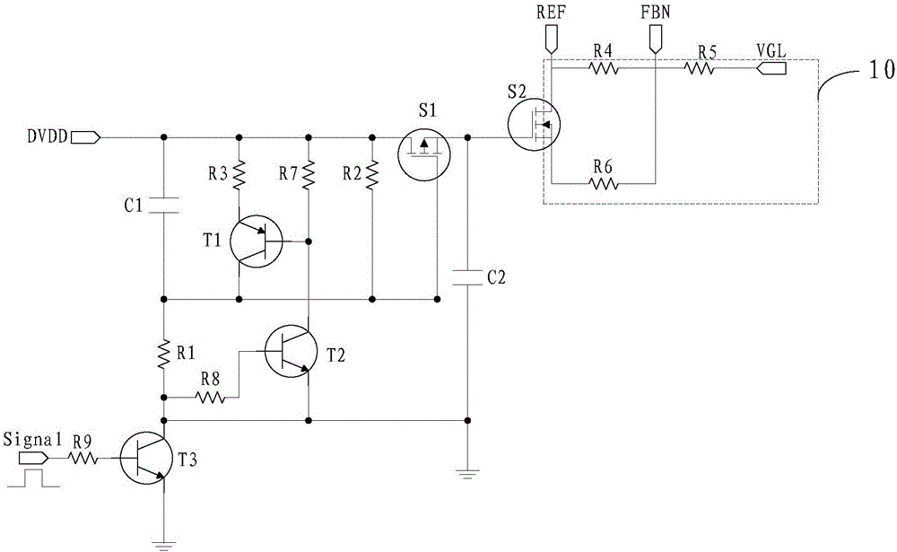
[0054] refer to figure 1 , shows a power-on delay circuit according to an embodiment of the present invention. The delay circuit includes a first switch tube S1, a second switch tube S2, a first capacitor C1 and a first resistor R1;

[0055] The source of the first switching tube S1 is connected to the power supply DVDD;

[0056] The first capacitor C1 is connected between the gate and the source of the first switching transistor S1;

[0057] The gate of the second switching tube S2 is connected to the drain of the first switching tube S1, and the drain and source of the second switching tube S2 are connected to the conversion circuit 10 for output voltage of the pixel off signal;

[0058] The first resistor R1 is connected between the ground terminal and the gate of the first switch S1, and the first resistor R1 is connected in series with the first capacitor C1;

[0059] The power supply DVDD charges the first capacitor C1 through the first resistor R1, the first switch t...

Embodiment 2

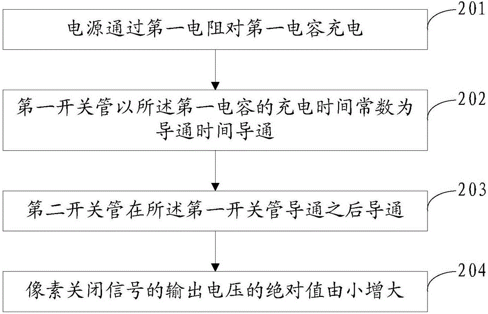
[0094] refer to figure 2 , shows a flowchart of steps of a method for delaying power-on according to an embodiment of the present invention. The method is applied to the power-on delay circuit described in Embodiment 1, including:

[0095] Step 201, the power supply charges the first capacitor through the first resistor.

[0096] In this embodiment, the power supply DVDD, the first capacitor C1, the first resistor R1 and the ground terminal are connected in series to form a charging path, and the power supply DVDD charges the first capacitor C1 through the first resistor R1.

[0097] Step 202, the first switch tube is turned on with the charging time constant of the first capacitor as the conduction time.

[0098]In this embodiment, the first capacitor C1 is connected between the gate and the source of the first switching tube S1, the power supply DVDD charges the first capacitor C1 through the first resistor R1, and the power of the first capacitor C1 gradually increases, ...

Embodiment 3

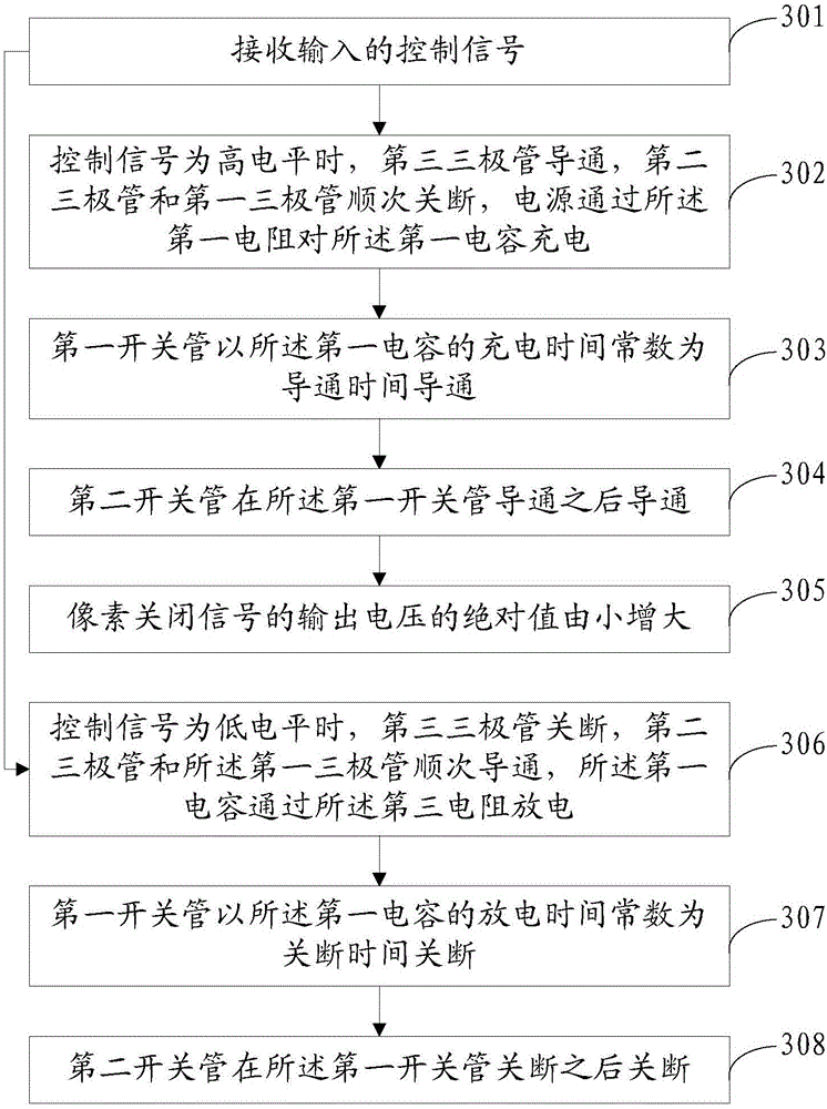
[0105] refer to image 3 , shows a flowchart of steps of a method for delaying power-on according to an embodiment of the present invention. The method is applied to the power-on delay circuit described in Embodiment 1, including:

[0106] Step 301, receiving an input control signal.

[0107] In this embodiment, the first triode T1 , the second triode T2 and the third triode T3 form a turn-off branch, so that the first capacitor C1 can be quickly discharged when the first switch S1 is turned off. The first transistor T1 can be a PNP transistor, and the turn-on threshold voltage of the PNP transistor is negative. The second transistor T2 and the third transistor T3 can be NPN transistors, and the turn-on threshold voltage of the NPN transistor is positive.

[0108] The base of the third transistor T3 is connected to the control signal terminal to receive the input control signal.

[0109] Step 302, when the control signal is at a high level, the third triode is turned on, th...


PUM


Abstract

The invention provides a power on delay circuit and method; the delay circuit comprises a first switch tube, a second switch tube, a first capacitor and a first resistor; the source electrode of the first switch tube is connected with a power supply; the first capacitor is connected between the grid electrode and the source electrode of the first switch tube; the grid electrode of the second switch tube is connected with the drain electrode of the first switch tube; the drain electrode and the source electrode of the second switch tube are connected with a conversion circuit of the output voltage of a pixel close signal; the first resistor is connected between the grounding end and the grid electrode of the first switch, and connected in series with the first capacitor; the power supply charges the first capacitor through the first resistor; the first and second switch tubes are conducted in order when the capacitor is charged, and the absolute value of the output voltage of the pixel close signal rises when the capacitor is charged. By using the method and circuit, the pixel quantity of light is weak when a black matrix charges the capacitor in the pixel in a start up process, and the quantity of light can be even reduced to a human eye undistinguishable level, so a user cannot notice the display panel whitening phenomenon.

Description

technical field [0001] The invention relates to the technical field of TFT-LCD, in particular to a power-on delay circuit and method. Background technique [0002] TFT-LCD (Thin Film Transistor-Liquid Crystal Display) is currently the mainstream display product. In recent years, major panel manufacturers have been expanding their production scale. With the popularity of smart phones and TVs, the market demand has increased in recent years. Improving production efficiency and producing high-quality backsheets is the key to dominating the market. [0003] In a TFT-LCD display panel, one pixel corresponds to a black matrix (black matrix, BM), and the material of the black matrix is ​​usually a slightly conductive material with low impedance. The black matrix at the edge of the display panel is very close to the signal lines that control the clock signal and pixel off signal of the display panel. When the power is turned on, power is applied to the signal line of the clock sig...

Claims


Application Information

Patent Timeline
Patent Type & Authority Applications(China)
IPC IPC(8): H03K17/284H03K17/28
CPCH03K17/28H03K17/284
Inventor 王光兴张斌孙含嫣董殿正张强张衎陈鹏名
Owner BOE TECH GRP CO LTD
Why Eureka
Try Eureka