Heat treating equipment and method for semiconductor chip
A technology for heat treatment equipment and semiconductors, which is used in semiconductor/solid-state device manufacturing, electrical components, circuits, etc., and can solve problems such as the inability to accurately measure the oxygen content of the reaction chamber and the inability to ensure the production quality of silicon wafers, and achieve the goal of ensuring production quality. Effect
- Summary
- Abstract
- Description
- Claims
- Application Information
AI Technical Summary
Problems solved by technology
Method used
Image

Examples
Embodiment Construction
[0028] The specific implementation manners of the present invention will be further described in detail below in conjunction with the accompanying drawings and embodiments. The following examples are used to illustrate the present invention, but are not intended to limit the scope of the present invention.
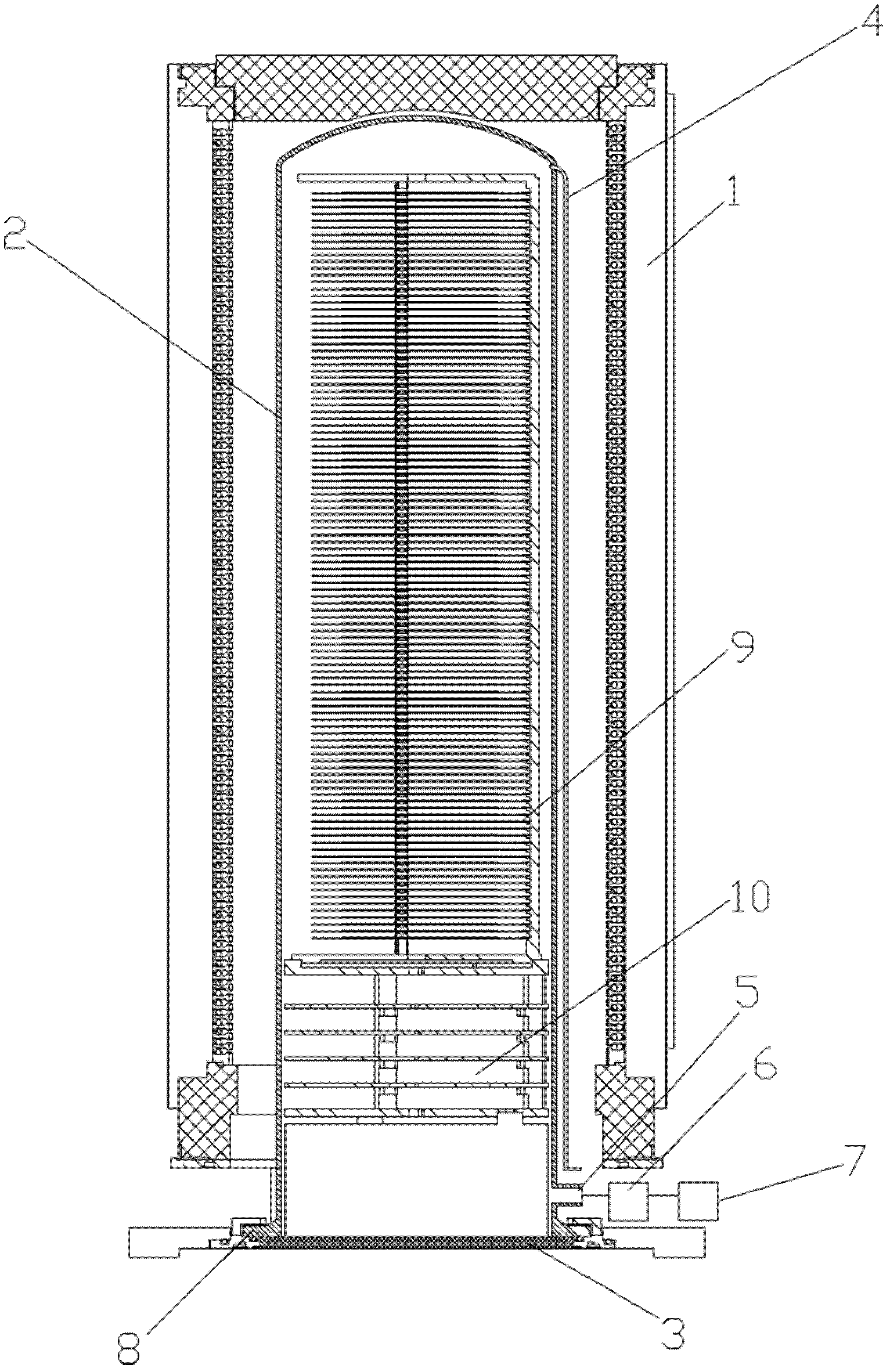
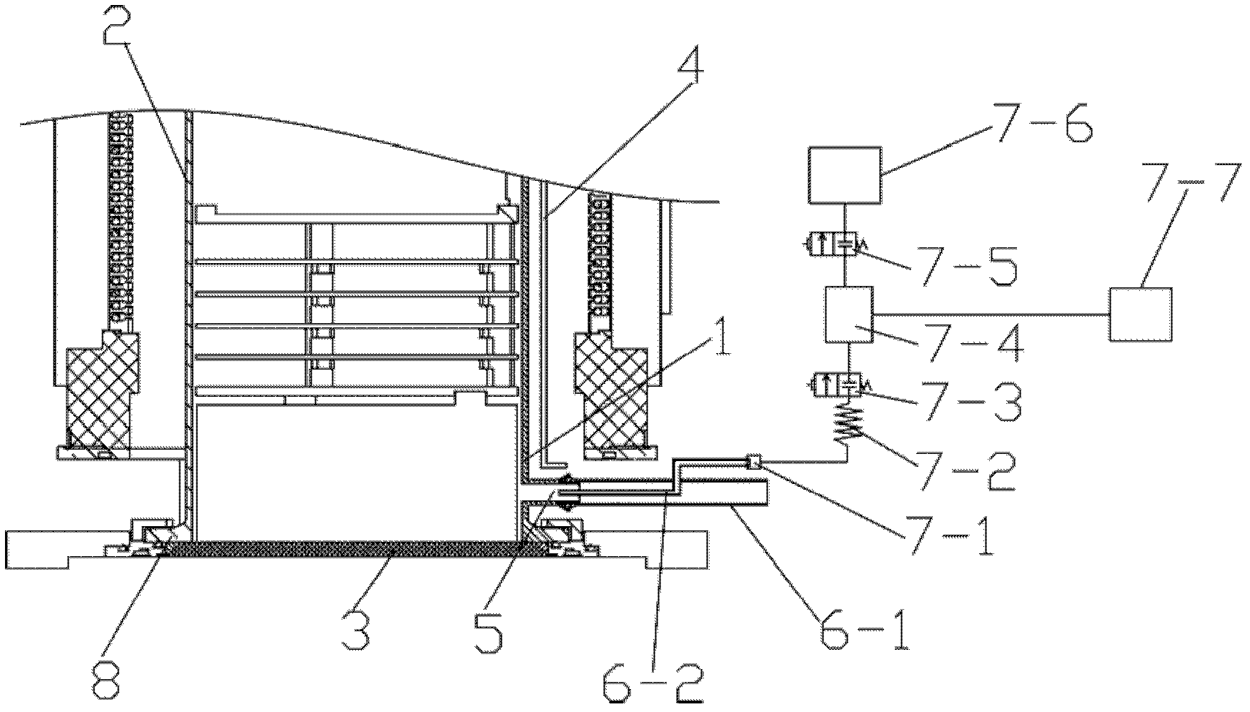
[0029] figure 1 It is a structural schematic diagram of a semiconductor wafer heat treatment equipment according to an embodiment of the present invention, see figure 1 , the heat treatment equipment includes: a heater 1, a process pipe 2, a sealing plate 3, an air inlet pipe 4, an exhaust pipe 5, a gas collection unit 6 and an oxygen content measurement unit 7, and the mouth of the process pipe 2 is vertically downward , the process tube 2 is partly placed in the heater 1, and the outer edge of the nozzle of the process tube 2 is provided with a flange 8 (the process tube 2 and the flange 8 can be integrally formed or processed separately, this In the embodiment, prefer...
PUM
 Abstract
Description
Claims
Application Information
 - R&D
- Intellectual Property
- Life Sciences
- Materials
- Tech Scout
- Unparalleled Data Quality
- Higher Quality Content
- 60% Fewer Hallucinations
Browse by: Latest US Patents, China's latest patents, Technical Efficacy Thesaurus, Application Domain, Technology Topic, Popular Technical Reports.
© 2025 PatSnap. All rights reserved.Legal|Privacy policy|Modern Slavery Act Transparency Statement|Sitemap|About US| Contact US: help@patsnap.com