Method for manufacturing through-hole prior copper through interconnection

A manufacturing method, through-hole priority technology, applied in semiconductor/solid-state device manufacturing, electrical components, circuits, etc., can solve problems such as complex metal interconnection forming process, achieve the effect of increasing production output and reducing costs

Active Publication Date: 2013-01-16
SHANGHAI HUALI MICROELECTRONICS CORP
View PDF4 Cites 3 Cited by
  • Summary
  • Abstract
  • Description
  • Claims
  • Application Information

AI Technical Summary

Problems solved by technology

[0007] However, the forming process of via-first dual damascene metal interconnection includes via photolithography-via etching-trench photolithography-trench etching

Method used


Image

  • Method for manufacturing through-hole prior copper through interconnection
  • Method for manufacturing through-hole prior copper through interconnection
  • Method for manufacturing through-hole prior copper through interconnection

Examples


Embodiment Construction

[0023] In order to make the content of the present invention clearer and easier to understand, the content of the present invention will be described in detail below in conjunction with specific embodiments and accompanying drawings.

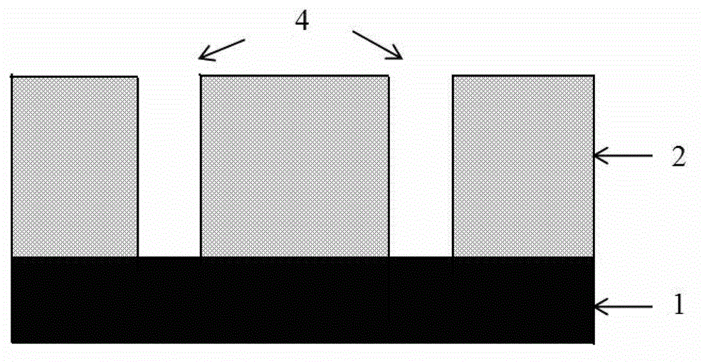
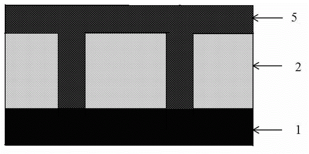
[0024] Figure 3A-Figure 3G A method for fabricating a via-first copper interconnection according to an embodiment of the present invention is schematically shown.

[0025] Such as Figure 3A-Figure 3G As shown, according to the embodiment of the present invention, the method for manufacturing via-first copper interconnection includes:

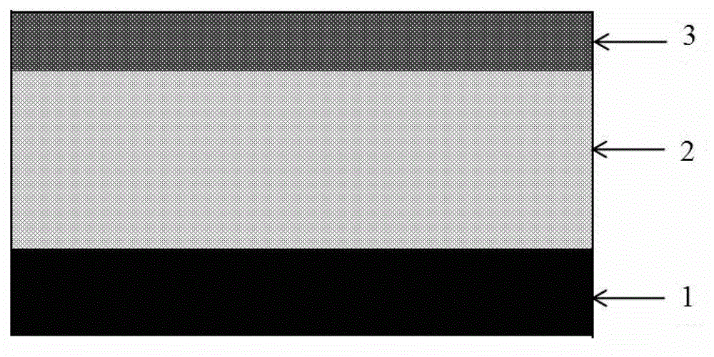
[0026] The first step is to first deposit a dielectric layer on the substrate silicon wafer 1, more specifically, deposit a low-k value dielectric layer 2; subsequently, coat a first photoresist 3 on the low-k value dielectric layer 2, The resulting structure is as Figure 3A shown.

[0027] Wherein, the first photoresist may be a photoresist capable of forming a hard film, preferably, a photoresist containi...


PUM


Abstract

The invention provides a method for manufacturing a through-hole prior copper through interconnection. The manufacturing method comprises the following steps: firstly, depositing a medium layer on a substrate silicon chip, and coating first photoresist on the medium layer; secondly, completing exposure and development so as to form a through-hole structure in a photoresist film; thirdly, heating and curing the through-hole structure, then coating cross-linking materials on the first photoresist and curing a through-hole structure diaphragm in the first photoresist, forming an isolating membrane insoluble in second photoresist, and then removing the cross-linking materials; fourthly, coating the second photoresist on the first cured photoresist; fifthly, completing the exposure and development and forming a metal groove structure of the through-hole structure in the second photoresist film; sixthly, completing etching so as to transfer the through hole and the metal groove structure in the photoresist into the medium layer; and seventhly, carrying out metal deposition and metal chemical machinery grinding so as to complete the wire metal and through-hole metal filling.

Description

technical field [0001] The present invention relates to a semiconductor manufacturing process, and more particularly, the present invention relates to a method for manufacturing via-hole-preferential copper interconnection. Background technique [0002] As the integration level of semiconductor chips continues to increase, the feature size of transistors continues to shrink. After entering the 130nm technology node, limited by the high resistance characteristics of aluminum, copper interconnection gradually replaces aluminum interconnection and becomes the mainstream of metal interconnection. [0003] Since the copper dry etching process is not easy to realize, the manufacturing method of the copper wire cannot be obtained by etching the metal layer like the aluminum wire. The widely used manufacturing method of copper wire is damascene technology called damascene process. [0004] Damascus damascene copper interconnects can be realized through a variety of process methods...

Claims


Application Information

Patent Timeline
IPC IPC(8): H01L21/768
Inventor 毛智彪
Owner SHANGHAI HUALI MICROELECTRONICS CORP
Why Eureka
Try Eureka