
Semiconductor device and manufacturing method thereof

A manufacturing method and semiconductor technology, applied in the fields of semiconductor/solid-state device manufacturing, semiconductor devices, electrical components, etc., can solve the problem of not being able to distinguish whether the dopant is activated or not, and achieve the effect of shallow junction and high concentration of activated dopant.

Active Publication Date: 2016-06-01
SEMICONDUCTOR MANUFACTURING INTERNATIONAL (BEIJING) CORP
View PDF5 Cites 0 Cited by
  • Summary
  • Abstract
  • Description
  • Claims
  • Application Information

AI Technical Summary

Problems solved by technology

[0006] However, the inventors of the present invention have carried out in-depth research on this and found that the junction depth and active dopant concentration of the source and drain extension regions formed by ion implantation and laser melting / sub-melting annealing need to be further improved
Incidentally, although SIMS (Secondary Ion Mass Spectrometry) is commonly used to measure the dopant distribution after laser melting / submelting annealing, SIMS cannot tell whether the dopant is activated or not

Method used


Image

  • Semiconductor device and manufacturing method thereof
  • Semiconductor device and manufacturing method thereof
  • Semiconductor device and manufacturing method thereof

Examples


Embodiment Construction

[0036] Exemplary embodiments of the present invention are described in detail below with reference to the accompanying drawings. It should be noted that the following description is merely exemplary in nature. The components, steps, numerical values ​​and the like set forth in the embodiments do not limit the scope of the present invention unless otherwise specifically stated. Additionally, techniques, methods and devices known to those skilled in the art may not be discussed in detail but are intended to be part of the description where appropriate.

[0037] The present invention will be described below by taking a transistor as an example. It is to be noted that the present invention is applicable not only to PMOS transistors but also to NMOS transistors, ie to CMOS transistors. In addition, the present invention can also be applied to other semiconductor devices, including replacement gate (RMG, ReplacementGate) devices (such as finFET) and the like.

[0038] The followi...


PUM


Abstract

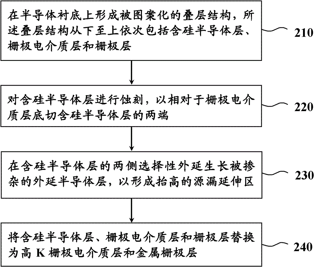
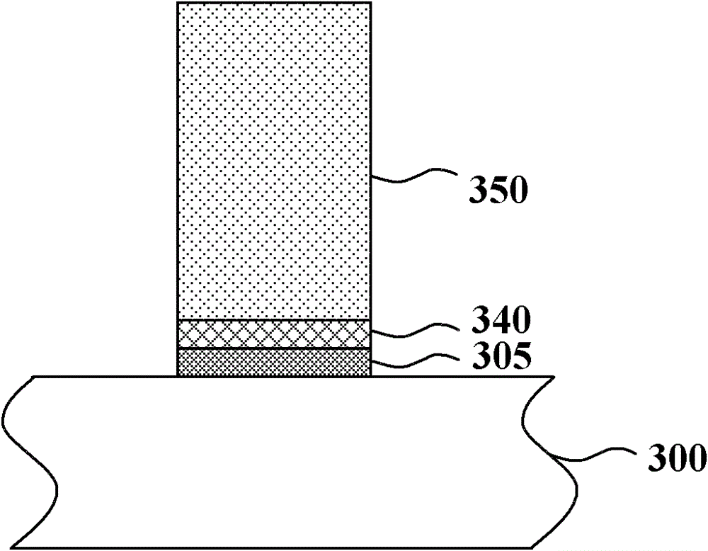
The invention relates to a semiconductor device and a manufacturing method thereof. The semiconductor device comprises a patterned laminated structure and doped epitaxial semiconductor layers, wherein the patterned laminated structure is formed on a semiconductor substrate; the laminated structure comprises a silicon containing semiconductor layer, a gate dielectric layer and a gate layer in sequence from bottom to top; the doped epitaxial semiconductor layers selectively and epitaxially grow on two sides of the silicon containing semiconductor layer; and the epitaxial semiconductor layers form raised source and drain extension regions. According to the invention, shallow junction depths (or small thickness) of the source and drain extension regions and high concentration of an activated doping agent can be advantageously achieved.

Description

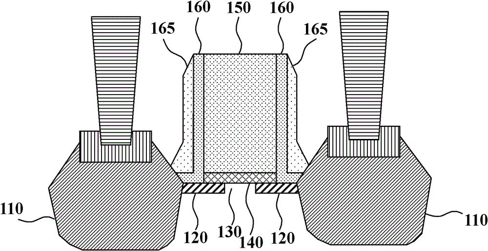
technical field [0001] The present invention relates to a semiconductor device and a method of manufacturing the same. In particular, the present invention relates to semiconductor devices with epitaxial source and drain extensions and methods of manufacturing the same. Background technique [0002] Currently, millions of semiconductor devices are integrated to form very large scale integrated circuits. [0003] figure 1 A cross-sectional view of a conventional semiconductor device (transistor) is shown. A transistor generally includes a gate dielectric layer 140 on a semiconductor substrate and a gate layer 150 on the gate dielectric layer 140 . Sidewall spacers 160 and 165 are formed on sidewalls of the gate dielectric layer 140 and the gate layer 150 . The transistor generally further includes a pair of source-drain regions 110 on both sides of the gate layer 150 . In addition, a pair of source-drain extension regions 120 are formed in the surface region of the semic...

Claims


Application Information

Patent Timeline
Patent Type & Authority Patents(China)
IPC IPC(8): H01L29/78H01L29/06H01L29/08H01L21/336
Inventor 三重野文健
Owner SEMICONDUCTOR MANUFACTURING INTERNATIONAL (BEIJING) CORP
Learn More