Method for locally burying PCB (Printed Circuit Board) daughter board in PCB

A printed circuit board and sub-board technology, which is applied in the direction of assembling printed circuits with electrical components, can solve problems such as size increase, large-scale equipment and process difficulties, and cost increase, so as to improve the bonding force and reduce the total cost of PCB design. The number of layers and the total thickness of the PCB, the effect of ensuring reliability

Inactive Publication Date: 2013-01-23
DONGGUAN SHENGYI ELECTRONICS
View PDF3 Cites 16 Cited by
  • Summary
  • Abstract
  • Description
  • Claims
  • Application Information

AI Technical Summary

Problems solved by technology

In order to realize the multi-functional hybrid structure of printed circuit boards, the existing design and production mainly adopt methods such as increasing the number of PCB layers, increasing the thickness of the PCB, and increasing the size of the PCB, which leads to the continuous increase in the size of the entire manufacturing equipment and the increase in cost , Excessive consumption of materials runs counter to the current direction of environmental protection, energy saving and emission reduction; at the same time, it brings the problem of "large size, high thickness" equipment and technology to PCB processing

Method used


Image

  • Method for locally burying PCB (Printed Circuit Board) daughter board in PCB
  • Method for locally burying PCB (Printed Circuit Board) daughter board in PCB
  • Method for locally burying PCB (Printed Circuit Board) daughter board in PCB

Examples


Embodiment Construction

[0027] In order to further illustrate the technical means adopted by the present invention and its effects, the following describes in detail in conjunction with preferred embodiments of the present invention and accompanying drawings.

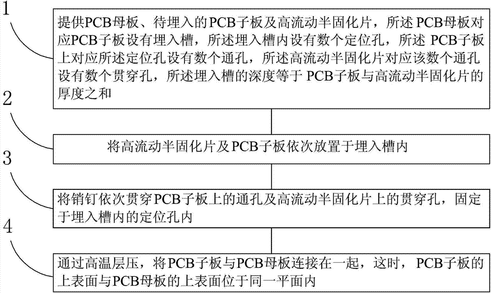
[0028] see Figure 1 to Figure 5 , the present invention provides a method for partially embedding a printed circuit board into a PCB sub-board, comprising the following steps:

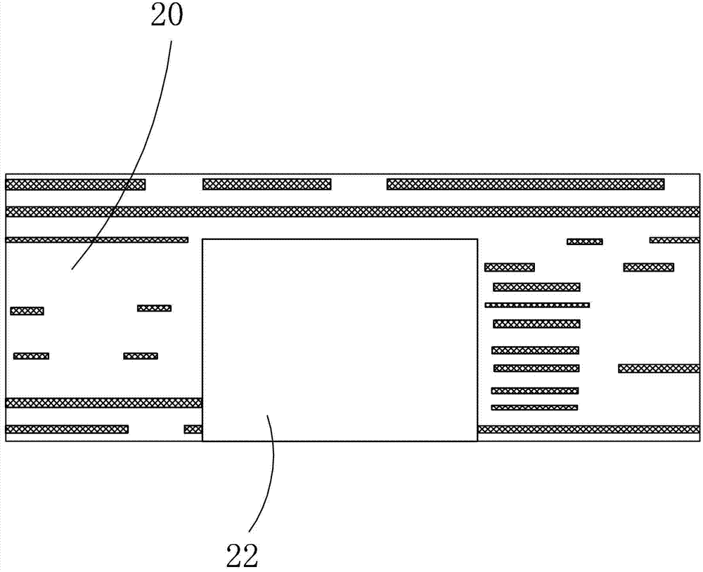
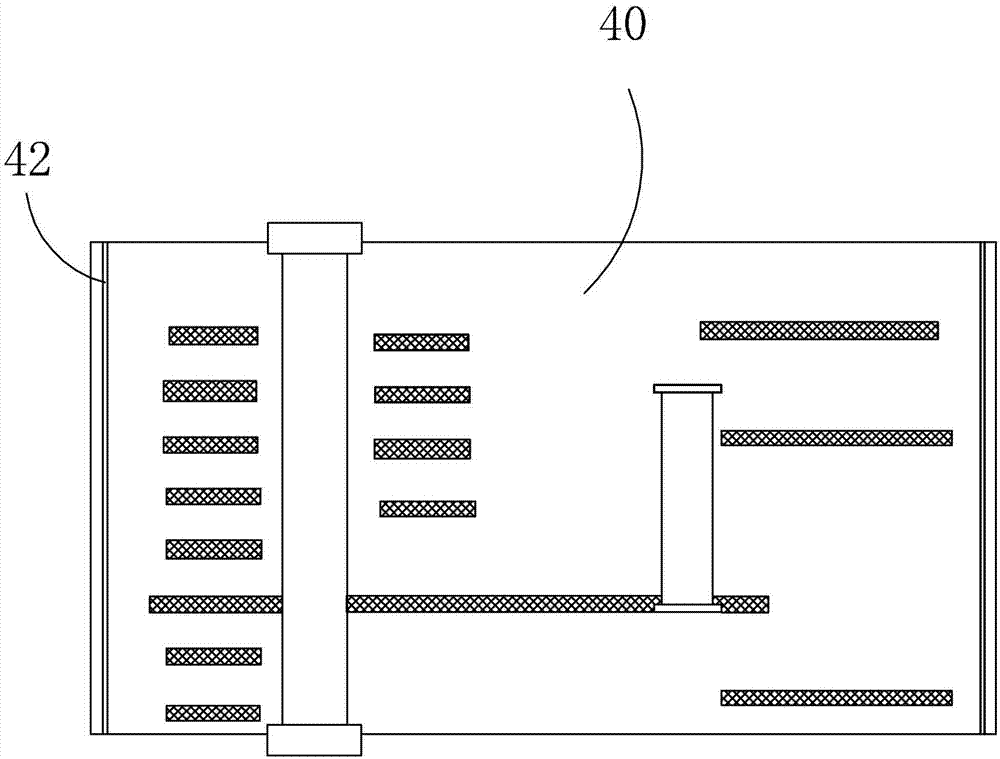
[0029] Step 1. Provide PCB motherboard 20, PCB sub-board 40 to be embedded and high-flow prepreg 60. The PCB motherboard 20 is provided with an embedding groove 22 corresponding to the PCB sub-board 40, and the embedding groove 22 is provided with several positioning holes (not shown), the PCB sub-board 40 is provided with several through holes 42 corresponding to the positioning holes, and the high flow prepreg 60 is provided with several through holes corresponding to the several through holes 42 (not shown in the figure). ), the depth of the buried groove 22 is eq...


PUM


Abstract

The invention provides a method for locally burying a PCB (Printed Circuit Board) daughter board in a PCB. The method comprises the following steps of: firstly, providing a PCB mother board, the PCB daughter board to be buried and a high-flow prepreg, wherein a burying groove corresponding to the PCB daughter board is arranged on the PCB mother board, a plurality of locating holes are formed in the burying groove, a plurality of through holes corresponding to the locating holes are formed on the PCB daughter board, a plurality of penetration holes corresponding to the plurality of through holes are formed on the high-flow prepreg, and the depth of the burying groove is equal to the thickness sum of the PCB daughter board and the high-flow prepreg; secondly, putting the high-flow prepreg and the PCB daughter board in the burying groove in sequence; thirdly, sequentially penetrating the through holes on the PCB daughter board and the penetration holes on the high-flow prepreg by pins, and then fixing the pins in the locating holes in the burying groove; and fourthly, performing high-temperature laminating to connect the PCB daughter board with the PCB mother board so as to ensure that the upper surface of the PCB daughter board is located in the same plane with the upper surface of the PCB mother board.

Description

technical field [0001] The invention relates to the field of printed circuit board (PCB) manufacturing, in particular to a method for partially embedding a printed circuit board using a high-flow prepreg into a PCB sub-board. Background technique [0002] Printed circuit board, also known as printed circuit board, printed circuit board, printed circuit board, often uses the English abbreviation PCB (Printed circuit board) or PWB (Printed wire board), is an important electronic component and a support for electronic components , is a provider of circuit connections for electronic components. Traditional circuit boards use the method of printing etching resist to make circuit lines and graphics, so they are called printed circuit boards or printed circuit boards. Due to the continuous miniaturization and refinement of electronic products, most of the current circuit boards are made by attaching etch resist (lamination or coating), after exposure and development, and then etch...

Claims


Application Information

Patent Timeline
Patent Type & Authority Applications(China)
IPC IPC(8): H05K3/36
Inventor 杜红兵陶伟吕红刚曾红
Owner DONGGUAN SHENGYI ELECTRONICS
Why Eureka
Try Eureka