

Ultrafast lens-free coherent electron diffraction imaging method and device
A technology of electron diffraction and imaging method, applied in circuits, discharge tubes, electrical components, etc., can solve the problems of limited time and space resolution, no high time resolution ability, etc., to achieve the effect of simple structure and cost reduction
- Summary
- Abstract
- Description
- Claims
- Application Information
AI Technical Summary
Problems solved by technology
Method used
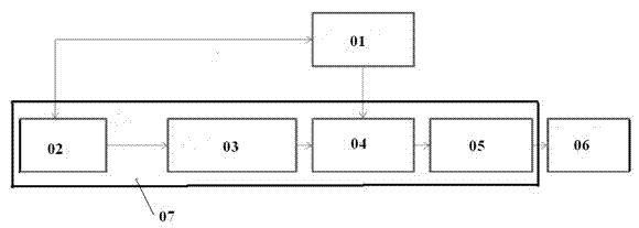
Image

Examples
Embodiment Construction
[0038] The present invention will be further described below in conjunction with the embodiments and accompanying drawings, but the protection scope of the present invention should not be limited thereby.
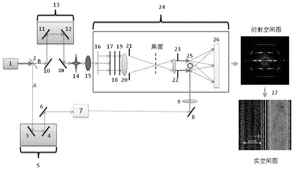
[0039] The ultra-fast lensless coherent electron diffraction imaging method of the present invention has the advantages of simple pulse electronic control system, and the spatial resolution is not restricted by the defocusing objective lens. It only needs a set of strong focusing magnetic lenses to focus the pulse electrons on the sample, without By defocusing the electromagnetic lens, ultra-high time and ultra-high spatial resolution in real space can be realized. This method is very easy to combine with MeV ultrafast electron diffraction, but this method has extremely high requirements on the coherence of the pulsed electron beam. The coherence of the pulsed electron beam and the focused electron spot size determine the spatial resolution of the present invention.
[004...
PUM
 Abstract
Description
Claims
Application Information