Method for preparing substrate with buried insulation layers by selective etching

An insulating buried layer and selective technology, which is applied in the manufacture of semiconductor/solid-state devices, electrical components, circuits, etc., can solve the problems of difficult control of corrosion and poor uniformity of silicon on the top layer of SOI substrate, so as to achieve accurate and controllable thickness and avoid causing Effect of damage and uniform thickness

Inactive Publication Date: 2013-01-30
SHANGHAI SIMGUI TECH +1
View PDF7 Cites 11 Cited by
  • Summary
  • Abstract
  • Description
  • Claims
  • Application Information

AI Technical Summary

Problems solved by technology

The problem with conventional methods is that during the etching process, the etching is not easy

Method used


Image

  • Method for preparing substrate with buried insulation layers by selective etching
  • Method for preparing substrate with buried insulation layers by selective etching
  • Method for preparing substrate with buried insulation layers by selective etching

Examples


Embodiment Construction

[0015] Next, a detailed description of a method for preparing a substrate with an insulating buried layer by selective etching according to the present invention will be described in detail with reference to the accompanying drawings.

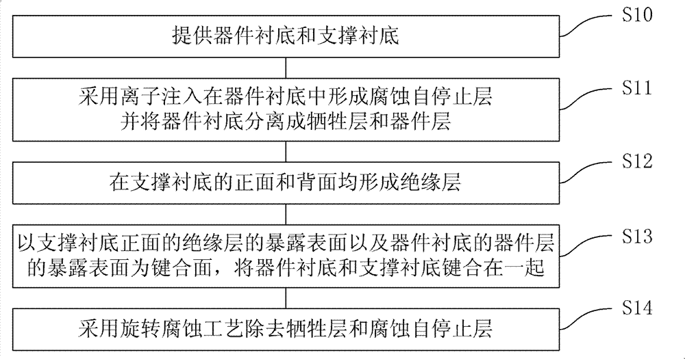
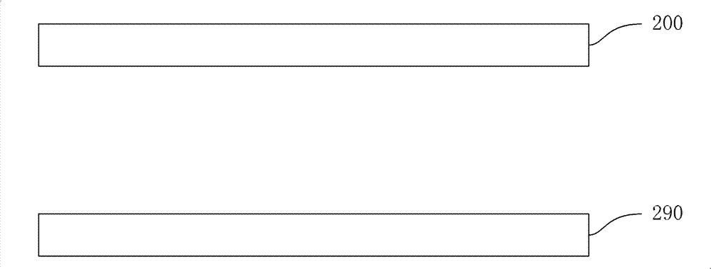
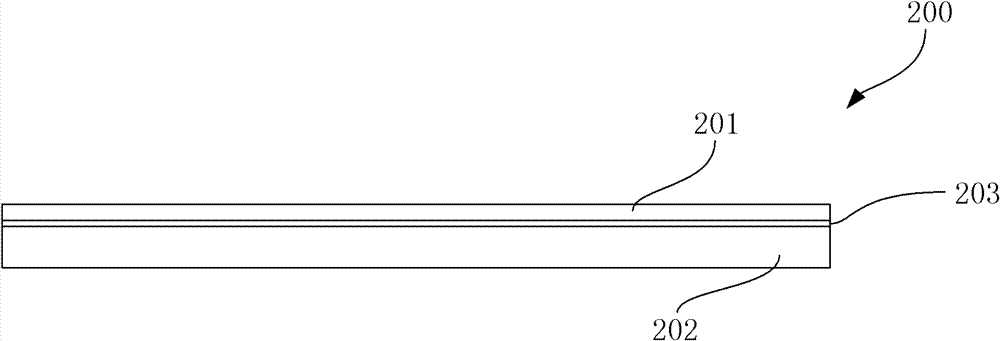
[0016] attached figure 1 Shown is a flow chart of the implementation steps of the method described in the specific embodiment of the present invention, including: step S10, providing a device substrate and a supporting substrate; step S11, using ion implantation to form an etching self-stopping layer in the device substrate, and The device substrate is separated into a sacrificial layer and a device layer; step S12, forming an insulating layer on the front and back sides of the supporting substrate; step S13, exposing the exposed surface of the insulating layer on the front side of the supporting substrate and the device layer of the device substrate The surface is a bonding surface, and the device substrate and the supporting substrate are bon...


PUM


Abstract

The invention provides a method for preparing a substrate with buried insulation layers by selective etching. The method includes the steps: providing a device substrate and a support substrate; forming an etching self-stopping layer on the device substrate by ion implantation, and separating the device substrate into a sacrificial layer and a device layer; forming insulation layers on the front side and the back side of the support substrate; bonding the device substrate and the support substrate together by using the exposed surface of the insulation layer on the front side of the support substrate and the exposed surface of the device layer of the device substrate as bonding surfaces; and removing the sacrificial layer and the etching self-stopping layer by the whirl etching process so as to form the substrate composed of the device layer, the insulation layers and the support substrate and provided with the buried insulation layers.

Description

technical field [0001] The invention relates to a method for preparing a silicon material on an insulator, in particular to a method for preparing a substrate with an insulating buried layer by selective etching. Background technique [0002] Compared with bulk silicon devices, silicon-on-insulator (SOI) devices have the advantages of high speed, low driving voltage, high temperature resistance, low power consumption, and radiation resistance. rapid development. According to the thickness of the top silicon thin layer, SOI materials can be divided into two categories: thin film SOI (top silicon is usually less than 1 μm) and thick film SOI (top silicon is usually greater than 1 μm). 95% of the applications in the thin film SOI market are concentrated in 8 inches and 12 inches, and the vast majority of users are leaders in cutting-edge microelectronics technology, such as IBM, AMD, Motorola, Intel, UMC, TSMC, OKI, etc. The current suppliers are Shin-Etsu (SEH) of Japan, Soi...

Claims


Application Information

Patent Timeline
IPC IPC(8): H01L21/02H01L21/762H01L21/84
Inventor 魏星曹共柏张苗张峰王曦
Owner SHANGHAI SIMGUI TECH
Why Eureka
Try Eureka