Semiconductor device and manufacturing method thereof

A manufacturing method and semiconductor technology, applied in the direction of semiconductor/solid-state device manufacturing, semiconductor devices, transistors, etc., can solve the problems of reducing device reliability and readout signal distribution, so as to improve device storage effect, increase tunneling current, and improve Effect of programming current vs. efficiency

Active Publication Date: 2013-01-30
INST OF MICROELECTRONICS CHINESE ACAD OF SCI
View PDF4 Cites 4 Cited by
  • Summary
  • Abstract
  • Description
  • Claims
  • Application Information

AI Technical Summary

Problems solved by technology

However, starting from sub-40nm NAND Flash, for example, as the feature size of the device continues to shrink, the coupling effect of adjacent memory cells becomes more and more serious. Therefore, it is necessary to continuously increase the P / E (program / erase) voltage of the device to improve efficiency, but thus Reduce the reliability of the device and the distribution of the readout signal, causing a vicious circle

Method used


Image

  • Semiconductor device and manufacturing method thereof
  • Semiconductor device and manufacturing method thereof
  • Semiconductor device and manufacturing method thereof

Examples


Embodiment Construction

[0035] One or more aspects of embodiments of the invention are described below with reference to the drawings, wherein like reference numerals generally refer to like elements throughout. In the following description, for purposes of explanation, numerous specific details are set forth in order to provide a thorough understanding of one or more aspects of the embodiments of the invention. It may be apparent, however, to one skilled in the art that one or more aspects of the embodiments of the invention may be practiced with a lesser degree of these specific details.

[0036] In addition, although a particular feature or aspect of an embodiment is disclosed in terms of only one of some implementations, such feature or aspect may be combined with other implementations that may be desirable and advantageous for any given or particular application. One or more other features or aspects of .

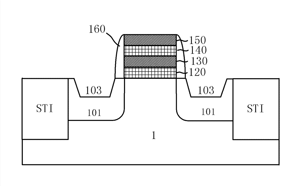
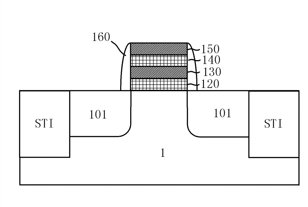
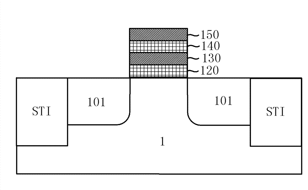
[0037] According to an exemplary manufacturing method of a semiconductor device accordin...


PUM


Abstract

The invention relates to a manufacturing method of a semiconductor device, which comprises a tunneling dielectric layer, a memory dielectric layer, a gate dielectric layer and a gate layer which are sequentially formed on a semiconductor substrate of a first semiconductor material; patterning the tunneling dielectric layer, memory dielectric layer, gate dielectric layer and gate layer to form a gate lamination body; forming trenches in the semiconductor substrate on both sides of the gate lamination body; and filling a second semiconductor material, which is different from the first semiconductor material, in the trenches, and meanwhile, covering the dielectric layer on the whole device. The surface energy level is changed through the stress generated by the second semiconductor material and the covering dielectric layer, thereby enhancing the tunneling current and improving the memory effect of the device.

Description

technical field [0001] The present invention relates to a semiconductor device and a manufacturing method thereof, and more particularly, to a storage device and a manufacturing method thereof. Background technique [0002] Memory devices are used for internal or external storage of electronic components including, but not limited to, computers, digital cameras, cell phones, MP3 players, personal digital assistants, video game consoles, and other devices. There are different types of memory devices, including volatile memory and nonvolatile memory. Volatile memory devices, such as, for example, random access memory (RAM), require a steady current to retain their contents. Nonvolatile memory devices retain or store information even when power to electronic components is terminated. For example, a read only memory (ROM) may hold instructions for operating an electronic device. Electrically Erasable Programmable Read-Only Memory (EEPROM) is a type of nonvolatile read-only me...

Claims


Application Information

Patent Timeline
Patent Type & Authority Applications(China)
IPC IPC(8): H01L21/336H01L29/788H01L29/792H01L29/06
CPCH01L29/66825H01L29/66833H01L29/792H01L29/7881
Inventor 殷华湘徐秋霞陈大鹏
Owner INST OF MICROELECTRONICS CHINESE ACAD OF SCI
Why Eureka
Try Eureka