A p/n-type stacked resistive memory with spontaneous growth of metal nanocrystal particles
A technology of metal nanocrystals and resistive memory, which is applied in the direction of electrical components, can solve the problems of large randomness of nanocrystals, the size of conductive channels, the instability of quantity, and the difficulty of controlling the number and size of nanocrystals, so as to improve the controllability The effect of controlling the fluctuation of device voltage and current, and uniformity
- Summary
- Abstract
- Description
- Claims
- Application Information
AI Technical Summary
Problems solved by technology
Method used
Image
Examples
Embodiment 1
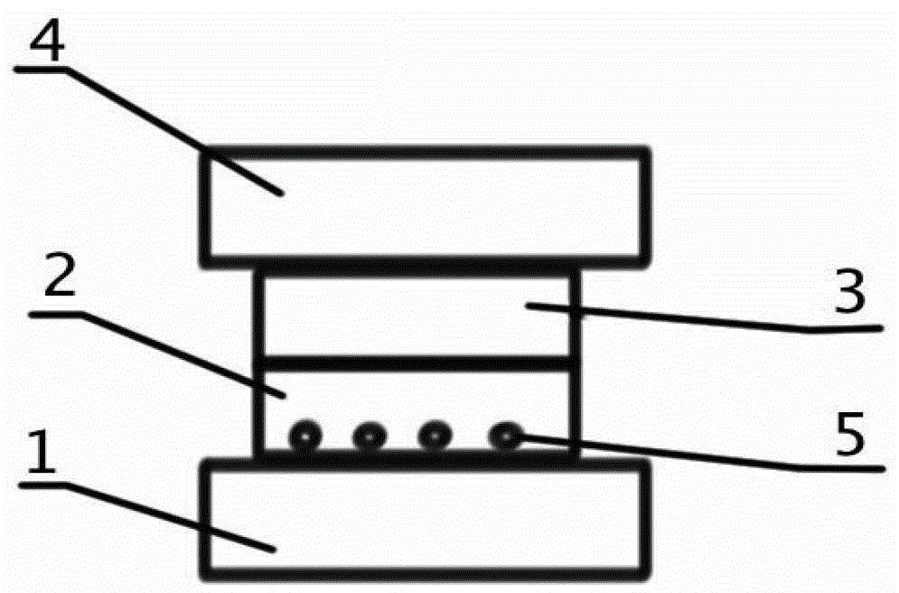
[0021] The resistive variable memory, as shown in the accompanying drawing, includes a lower electrode 1, an induction layer I2, an induction layer II3, an upper electrode 4, and an induction layer I2 in which metal nanocrystalline particles 5 are spontaneously formed; the lower electrode is made of 50nm copper metal, and the induction layer I use 100nm silicon dioxide doped with 3% phosphorus, and the induction layer II uses 100nm silicon dioxide doped with 3% boron; the upper electrode uses 50nm platinum metal.
[0022] The preparation steps of the resistive variable memory are as follows:
[0023] 1) Use PVD (physical vapor deposition) to deposit the lower electrode, which is 50nm thick metallic copper;
[0024] 2) Use PVD (physical vapor deposition) to deposit induction layer I with silicon dioxide doped with 3% phosphorus, and its thickness is 100nm;
[0025] 3) Use PVD (physical vapor deposition) to deposit induction layer II silicon dioxide doped with 3% boron, with a ...
Embodiment 2
[0029] The resistive variable memory, as shown in the accompanying drawing, includes a lower electrode 1, an induction layer I2, an induction layer II3, an upper electrode 4, and an induction layer I2 in which metal nanocrystalline particles 5 are spontaneously formed; the lower electrode is made of 50nm copper metal, and the induction layer 100nm titanium oxide is used for I, 100nm nickel oxide is used for the induction layer II; 50nm platinum metal is used for the upper electrode.
[0030] The preparation steps of the resistive variable memory are as follows:
[0031] 1) Use PVD (physical vapor deposition) to deposit the lower electrode, which is 50nm thick metallic copper;
[0032] 2) The induction layer I titanium oxide is deposited by DC magnetron sputtering method, the process parameters are 100W power, the working pressure is 1Pa, the oxygen partial pressure is 5%, the temperature is 300K, and its thickness is 100nm;
[0033] 3) The induction layer II nickel oxide is d...
PUM
| Property | Measurement | Unit |
|---|---|---|
| thickness | aaaaa | aaaaa |
| thickness | aaaaa | aaaaa |
Abstract
Description
Claims
Application Information
 - R&D
- Intellectual Property
- Life Sciences
- Materials
- Tech Scout
- Unparalleled Data Quality
- Higher Quality Content
- 60% Fewer Hallucinations
Browse by: Latest US Patents, China's latest patents, Technical Efficacy Thesaurus, Application Domain, Technology Topic, Popular Technical Reports.
© 2025 PatSnap. All rights reserved.Legal|Privacy policy|Modern Slavery Act Transparency Statement|Sitemap|About US| Contact US: help@patsnap.com

