
Method for manufacturing semiconductor device

A manufacturing method, semiconductor technology, applied in the direction of semiconductor devices, single semiconductor device testing, semiconductor/solid-state device components, etc., can solve the problem of lower pass rate of withstand voltage and achieve the effect of improving the pass rate

Inactive Publication Date: 2013-01-30
SUMITOMO ELECTRIC IND LTD
View PDF5 Cites 3 Cited by
  • Summary
  • Abstract
  • Description
  • Claims
  • Application Information

AI Technical Summary

Problems solved by technology

[0003] To increase the capacity (higher current) of power devices using SiC semiconductors, it is necessary to expand the chip area, but because the pass rate of withstand voltage is greatly reduced, only small-capacity chips are currently being put into practical use.

Method used


Image

  • Method for manufacturing semiconductor device
  • Method for manufacturing semiconductor device
  • Method for manufacturing semiconductor device

Examples


no. 1 Embodiment approach

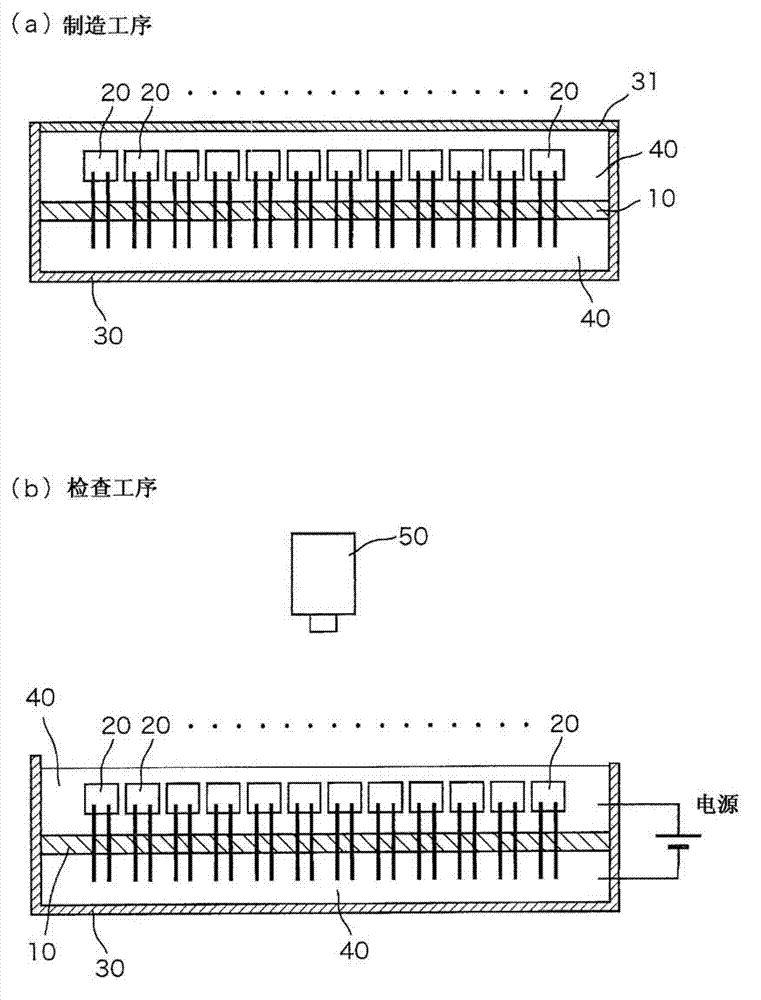
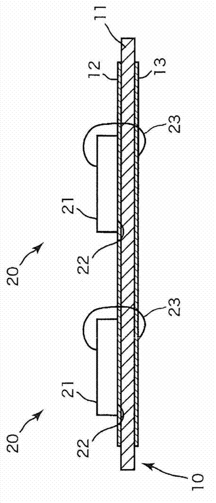
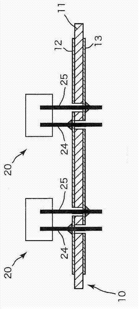
[0036] figure 1 It is an explanatory drawing explaining the outline of the manufacturing method of the semiconductor device of 1st Embodiment. The manufacturing method of the semiconductor device of the present embodiment includes: a mounting step ( figure 1 (a)), forming a circuit in which a plurality of SiC semiconductor chips 20 are connected in parallel on the mounting substrate 10; and the inspection process ( figure 1 (b)), it is checked whether the mounted SiC semiconductor chip 20 is defective.

[0037] The SiC semiconductor chip 20 is a small-capacity chip having a current capacity of about 1 to 10 A. By connecting a plurality of SiC semiconductor chips 20 in parallel on the mounting substrate 10 , a semiconductor device (for example, a power device) capable of increasing current is realized. The SiC semiconductor chips 20 have a size of about 2 mm square, and are arranged on the mounting substrate 10 at intervals of several millimeters in a straight line or in a m...

no. 2 Embodiment approach

[0060] In the first embodiment, a method of identifying a defective chip using a thermal imaging device 50 such as an infrared camera or an infrared microscope has been described, but as a mechanism for detecting heat generation in a defective chip, it is possible to use a method that changes color according to heat generation. Temperature-indicating materials such as temperature-indicating paper or temperature-indicating paint that have changed. In this embodiment, a method for identifying unqualified chips using temperature-indicating materials such as temperature-indicating paper or temperature-indicating paint is described.

[0061] In the second embodiment, the presence or absence of heat generation in each SiC semiconductor chip 20 is detected using a temperature indicating material such as temperature indicating paper or temperature indicating paint. Figure 6 It is an explanatory drawing explaining the outline of the manufacturing method of the semiconductor device of ...

no. 3 Embodiment approach

[0066] As a mechanism for detecting heat generation in defective chips, in addition to thermal imaging devices 50 such as infrared cameras and infrared microscopes, and temperature-indicating materials 60 such as temperature-indicating paper or temperature-indicating paint, temperature sensors using thermocouples, thermistors, etc. can also be used. . In this embodiment, a method of identifying a defective chip using a temperature sensor such as a thermocouple or a thermistor will be described.

[0067] In the third embodiment, the presence or absence of heat generation in each SiC semiconductor chip 20 is detected using a temperature sensor such as a thermocouple or a thermistor. Figure 7 It is an explanatory drawing explaining the outline of the manufacturing method of the semiconductor device of 3rd Embodiment. The manufacturing method of the semiconductor device of the third embodiment is the same as that of the first embodiment, and includes: a mounting step ( Figure ...


PUM


Abstract

Disclosed is a method for manufacturing a semiconductor device, wherein, in a step (S1), a plurality of SiC semiconductor chips are mounted on a mounting substrate, and in a step (S2), a voltage is applied to the SiC semiconductor chips on the mounting substrate. In a step (S3), in the state wherein the voltage is applied, a temperature distribution image of the mounting substrate surface is obtained using thermography and thermal image devices, such as an infrared microscope, and in a step (S5), whether there is a failure chip or not is determined by analyzing the image. In a step (S7), in the case (S5:YES) wherein the failure chip is contained in the mounting substrate, the failure chip is rejected by cutting the wiring of the failure chip. Consequently, the method for manufacturing a semiconductor chip using small-capacity chips is provided.

Description

technical field [0001] The present invention relates to a method of manufacturing a semiconductor device using a small-capacity chip. Background technique [0002] Silicon carbide (SiC) not only has excellent properties in hardness, heat resistance, and chemical stability, but also has attracted attention as a semiconductor material. In recent years, power devices using SiC semiconductors have been put into practical use. [0003] To increase the capacity (higher current) of power devices using SiC semiconductors, it is necessary to increase the chip area, but because the yield of withstand voltage is greatly reduced, only small-capacity chips are currently in practical use. [0004] A semiconductor device has been proposed in which a plurality of small-capacity chips are connected in parallel in order to realize a large current using the above-mentioned small-capacity chips (for example, refer to Patent Document 1). [0005] prior art literature [0006] patent documents ...

Claims


Application Information

Patent Timeline
IPC IPC(8): G01N25/72G01R31/26H01L25/07H01L25/18
CPCH01L23/24H01L2924/1033H01L22/20H01L2924/10272H01L2224/4824H01L24/48H01L2924/1304H01L2924/1203H01L2924/10254H01L25/072H01L2224/49111H01L22/10H01L22/14H01L2224/49175H01L2924/014H01L25/50H01L2924/12042H01L2924/00014H01L24/49H01L2924/00H01L2224/45099H01L2224/45015H01L2924/207G01N25/72G01R31/26H01L25/07H01L25/18
Inventor 初川聪
Owner SUMITOMO ELECTRIC IND LTD
Learn More