Device for shaping and collimating elliptic laser spots of semiconductor lasers

An elliptical spot and laser technology, applied in the field of optics, can solve the problems of large divergence angle, unrealized shaping, and many optical elements, and achieve the effect of less optical elements, small size, and meeting application requirements

Active Publication Date: 2013-02-06
SUZHOU INST OF NANO TECH & NANO BIONICS CHINESE ACEDEMY OF SCI
View PDF7 Cites 15 Cited by
  • Summary
  • Abstract
  • Description
  • Claims
  • Application Information

AI Technical Summary

Problems solved by technology

[0005] There are many patents on beam shaping of semiconductor lasers, such as CN200956493Y, CN2754113Y, CN101609212A and CN102313995A, etc., but the optical system involved either only shapes the elliptical spot into a symmetrical circle, the divergence angle is large, and the collimation eff

Method used


Image

  • Device for shaping and collimating elliptic laser spots of semiconductor lasers
  • Device for shaping and collimating elliptic laser spots of semiconductor lasers
  • Device for shaping and collimating elliptic laser spots of semiconductor lasers

Examples


Embodiment 1

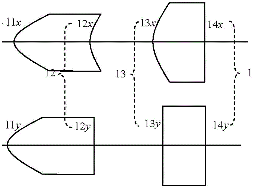
[0054] Embodiment 1 This embodiment adopts the above first kind of implementation scheme and figure 2 The lens shown is realized.

[0055] Since the diameter of the MEMS galvanometer is 1 mm, the beam section radius after the fast axis direction is collimated by the surface 11y ω 11y 0.5mm. In order to use Zemax to simulate the aspheric surface shape of surface 11, according to the law of paraxial optical propagation, firstly determine the radius of curvature of surface 11 and the distance from the beam waist to the apex of the surface. The specific calculation process is as follows:

[0056]

[0057]

[0058]

[0059]

[0060]

[0061] In the formula, ω is the beam section radius of the laser, and its subscript number (such as "11") represents the number of the surface, and the subscript " x ( y )" represents the slow axis (fast axis) direction, that is ω 11y is the beam section radius in the fast axis direction on the surface 11. ω 0 is the beam wais...

Embodiment 2

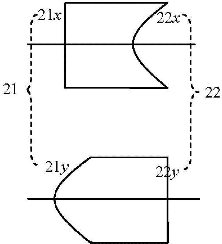
[0075] Embodiment 2 This embodiment adopts the above second implementation scheme and image 3 The lens shown is realized.

[0076] In this embodiment, the fast axis direction surface 21 y The calculation method of the radius of curvature is the same as in Example 1, namely r 21y = r 11y =0.715mm, d 0 =2.145mm, slow axis direction surface 21 x is flat. The light beam in the direction of the slow axis is collimated and passes through the surface 22 x to fulfill. Lens thickness and surface 22 x The formula for determining the radius of curvature is as follows:

[0077]

[0078]

[0079]

[0080] In this example, ω 11x =0.197mm, ω 12x =0.5mm, θ x =5 0 , n 0 =1, n =1.5, calculated d glass =5.206mm, r 22x =2.864mm.

[0081] The above parameters d 0 , d glass , r 21y、 r 22x As an initial parameter, the specific optimization process is similar to Embodiment 1, and the surface parameters of the two surfaces of the lens are obtained as follow...

Embodiment 3

[0085] Embodiment 3 This embodiment adopts the above third implementation scheme and Figure 4 The lens shown is realized.

[0086] In this embodiment, the first surface 31 of the first lens is the same as the first surface 11 of the first lens in Embodiment 1, namely r 31 = r 11 =0.715mm, d 0 =2.145mm. The formula for calculating the distance between the second surface 34 of the second lens in the direction of the slow axis and the first surface 35 of the third lens is as follows:

[0087]

[0088] In the formula, d 34-35 is the distance between the focal coincidence position between the surface 34 and the surface 35 and the surface 34 . The thickness of the first lens d 1 =5mm, second lens thickness d 1 =3mm, the distance between the first lens and the second lens is d 32-33 =2mm. Concrete optimization process is similar to embodiment 1, and the parameters of three lens surfaces that obtain are as follows:

[0089]

[0090] Using POP to analyze the opt...


PUM


Abstract

The invention discloses a device for shaping and collimating elliptic laser spots of semiconductor lasers, which comprises at least a non-rotational symmetric lens arranged on the propagation path of laser beams emitted by a semiconductor laser, the lens comprises a first surface and a second surface, the first surface is used for realizing the purpose of collimating laser beams propagated in the direction of a fast axis, and the second surface is used for carrying out beam expansion and collimation on laser beams propagated in the direction of a slow axis. The device disclosed by the invention has the advantages of less adopted optical elements, small size and capability of shaping and collimating elliptic laser spots, thereby fully meeting the application requirements of micro-projector optical systems of MEMS (micro-electro-mechanical system) galvanometers.

Description

technical field [0001] The invention specifically relates to a device for shaping and collimating an elliptical spot of a semiconductor laser, which is especially suitable for micro-optical systems requiring the upper limit of the spot size to be several mm, and for shaping an asymmetric elliptical beam output by a semiconductor laser into a circular beam , belonging to the field of optical technology. Background technique [0002] The miniaturization of the projector is one of the inevitable trends in the development of the projector, and the key to the miniaturization of the projector is the core display technology. The just-started MEMS projection technology has become one of the emerging display technologies that are expected to enter the embedded application market due to its outstanding advantages such as simple system, small size, low light loss rate, and high resolution. MEMS projection technology uses the optical design of the combination of laser light source and ...

Claims


Application Information

Patent Timeline
IPC IPC(8): G02B27/09G02B27/30G02B3/06
Inventor 李敏吴东岷
Owner SUZHOU INST OF NANO TECH & NANO BIONICS CHINESE ACEDEMY OF SCI
Why Eureka
Try Eureka