Address assignment method for data registers of distributed cache chipset

A data buffer and distributed buffer technology, applied in memory address/allocation/relocation, electrical digital data processing, instruments, etc. Problems such as limited foot resources

Active Publication Date: 2013-02-06
MONTAGE TECHNOLOGY CO LTD
View PDF3 Cites 7 Cited by
  • Summary
  • Abstract
  • Description
  • Claims
  • Application Information

AI Technical Summary

Problems solved by technology

[0004] The configuration of the above address pins undoubtedly increases the overall size of the chip and also affects the size of the entire distributed cache chipset
However, in order to enhance market competitiveness, the existing computers are light, thin and small as the ultimate goal, so the distributed cache chipset configured in the computer must also develop in this direction, resulting in the distributed cache chipset packaged in the distributed cache chipset. The pin resources of the data register are also limited

Method used


Image

  • Address assignment method for data registers of distributed cache chipset
  • Address assignment method for data registers of distributed cache chipset
  • Address assignment method for data registers of distributed cache chipset

Examples


no. 1 example

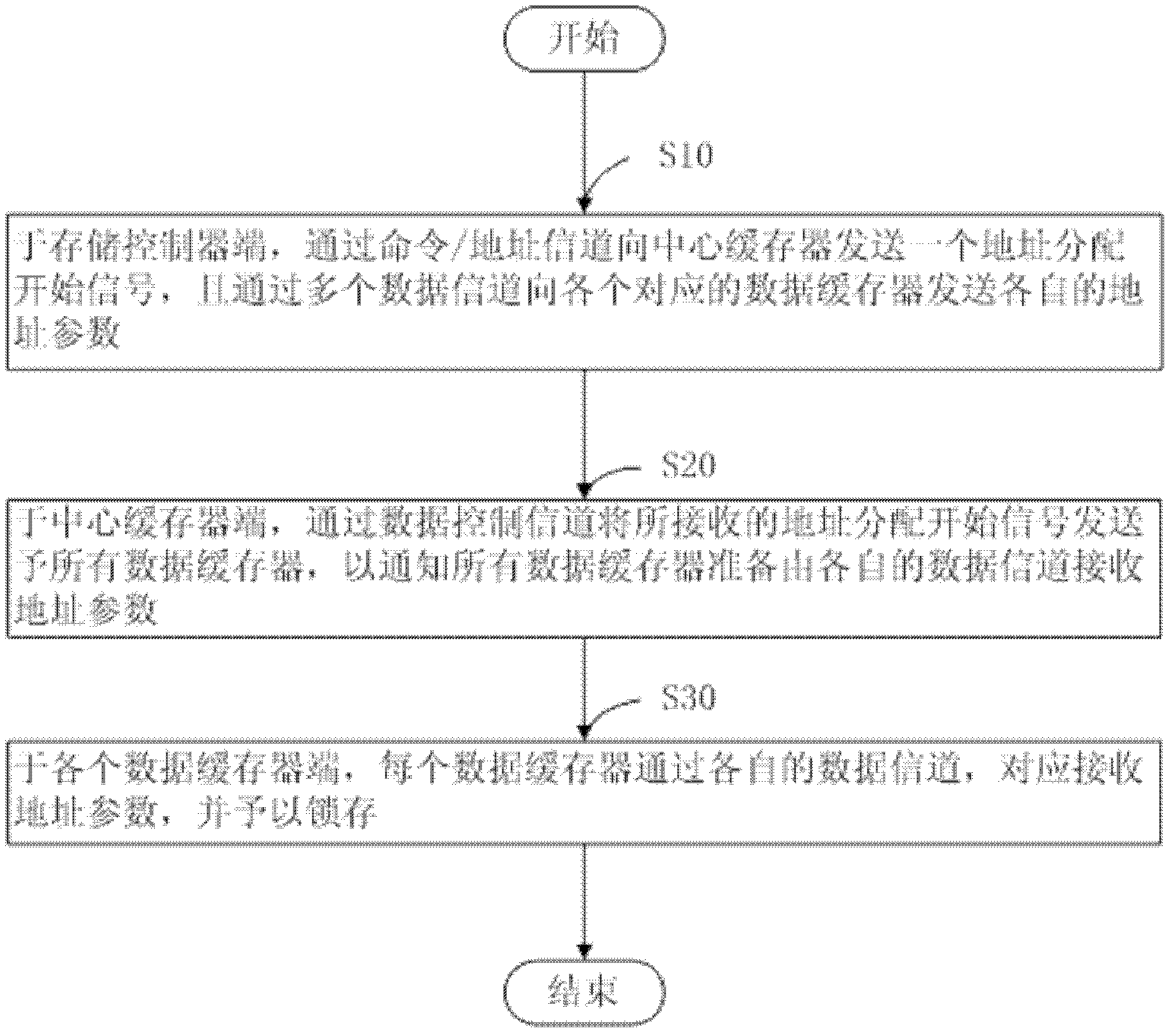
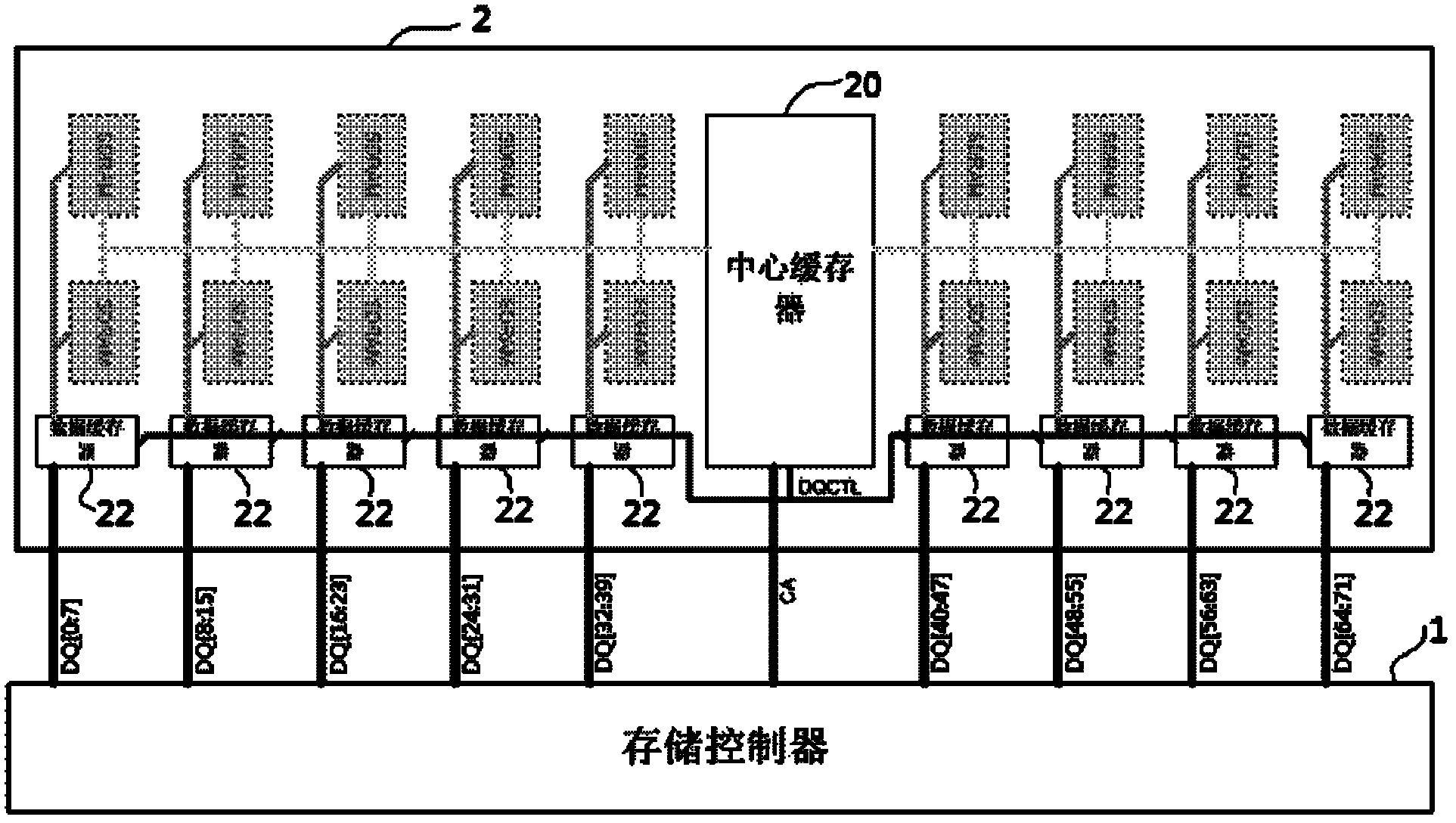
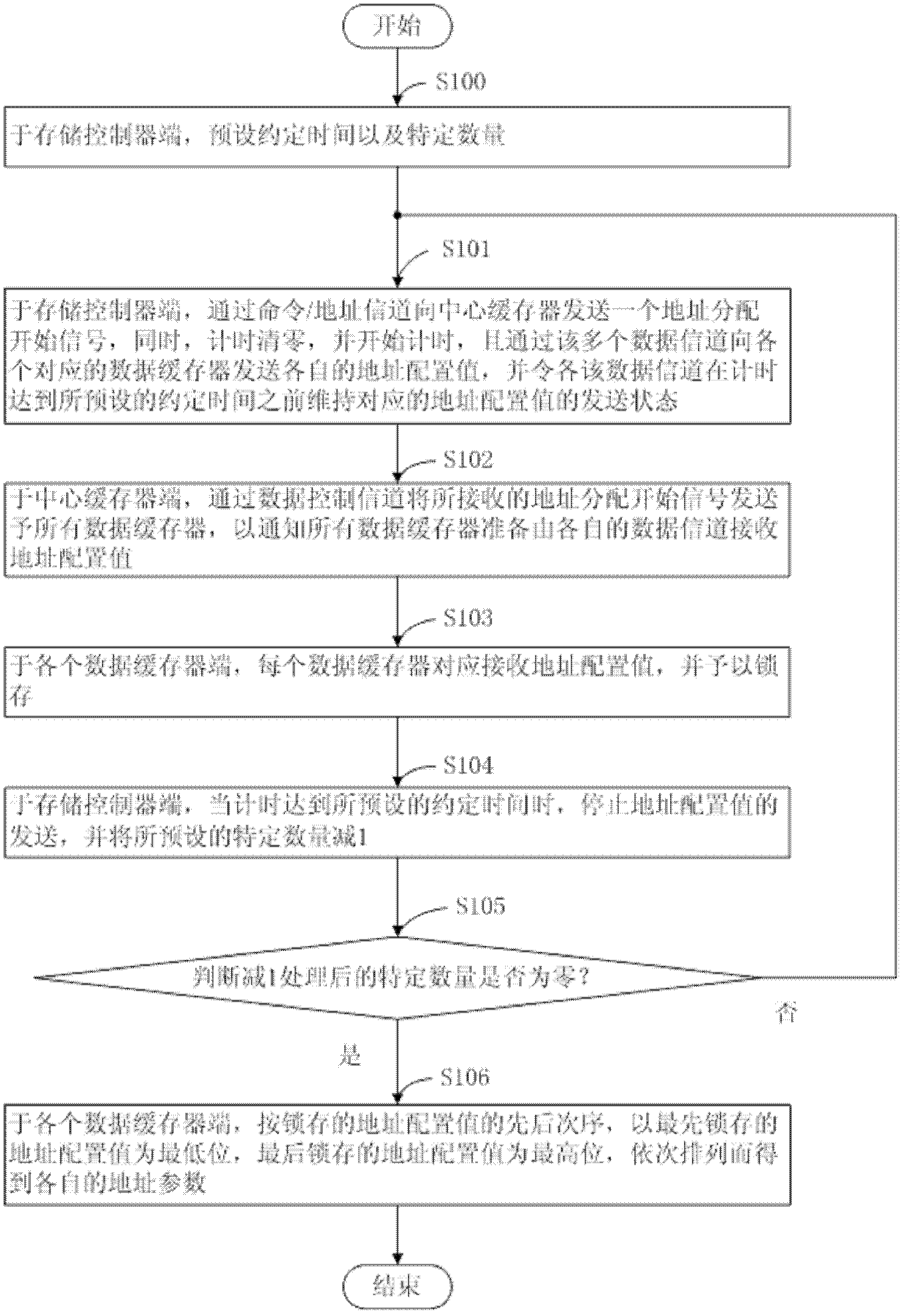
[0040] Preferably, see image 3 , is a schematic diagram showing the operation flow of the first embodiment of the address allocation method of the data buffer in the distributed cache chipset of the present invention. The following fit figure 2 The specific operation steps of the address allocation method of the data buffer in the distributed cache chipset of the present invention will be described in detail.

[0041] Firstly, step S100 is executed to preset an appointment time and a specific amount at the end of the storage controller 1 . Wherein, the appointed time is set to ensure that the data buffer 22 has enough time to receive and latch its address configuration value after receiving the address allocation start signal. Next, proceed to step S101.

[0042] In step S101, at the storage controller 1 end, an address allocation start signal is sent to the central buffer 20 through the command / address channel (CA), and at the same time, the timer is cleared and starts t...

no. 2 example

[0053] see Figure 4 , is a schematic diagram showing the operation flow of the second embodiment of the address allocation method of the data buffer in the distributed cache chipset of the present invention, wherein, the address of the data buffer in the distributed cache chipset of the previous embodiment distribution method (such as image 3 Shown) the same or similar steps are represented by the same or similar symbols, and detailed descriptions are omitted to make the description of this case clearer and easier to understand.

[0054] The biggest difference between the address assignment method of the data buffer in the distributed cache chipset of the second embodiment and the address assignment method of the data buffer in the distributed cache chipset of the first embodiment is that the first embodiment The address allocation method of the data buffer in the distributed cache chipset is at the storage controller side, and each sending state of the address configuratio...

no. 3 example

[0056] see Figure 5 , is a schematic diagram showing the operation flow of the third embodiment of the address allocation method of the data buffer in the distributed cache chipset of the present invention, wherein, the address of the data buffer in the distributed cache chipset of the previous embodiment distribution method (such as image 3 as well as Figure 4 Shown) the same or similar steps are represented by the same or similar symbols, and detailed descriptions are omitted to make the description of this case clearer and easier to understand.

[0057] The address assignment method of the data buffer in the distributed cache chipset of the third embodiment and the address assignment method of the data buffer in the distributed cache chipset of the first embodiment and the distributed cache chipset of the second embodiment The biggest difference in the address allocation method of the data buffer in the first embodiment and the second embodiment of the distributed cach...


PUM


Abstract

The invention relates to an address assignment method for data registers of a distributed cache chipset. The address assignment method includes: a memory controller informs a central register through a command/address channel to start address assignment, then the central register informs all the data registers through a data control channel to prepare to receive address parameters through respective data channels, and the data registers receive and latch respective address parameters from the memory controller through the data channels. The defect that the data registers need multiple extra address pins to assign respective address data in the prior art, and size simplification of the data registers and the overall distributed cache chipset is influenced accordingly can be overcome.

Description

technical field [0001] The invention relates to a data buffer address allocation technology, in particular to a data buffer address allocation method applied in a distributed buffer chipset (Distributed Buffer Chipset). Background technique [0002] Today's computer systems require higher and higher memory (usually SDRAM) capacity. More memory means greater load and reduced signal integrity, so the memory capacity is limited. In order to increase the memory capacity of the system, a low-load dual in-line memory group (Load Reduced DIMM, LRDIMM) is designed, which inserts a buffer (Buffer) between the storage controller (Memory Controller) and the memory (such as SDRAM) to cache all The information, including commands, addresses and data, is driven by the storage controller to several registers, and then each register drives several memories, so the memory capacity is improved. [0003] At present, the buffer of LRDIMM is not necessarily a single chip, and some are distribut...

Claims


Application Information

Patent Timeline
Patent Type & Authority Applications(China)
IPC IPC(8): G06F12/08
CPCG06F12/08G06F13/1673
Inventor 楚怀湘马青江
Owner MONTAGE TECHNOLOGY CO LTD
Why Eureka
Try Eureka